Hello,
I am attempting to program to a custom board using VS Code. I am using the Bluetooth beacon advertising example from BLE fundamentals Lesson 2 Exercise 1.
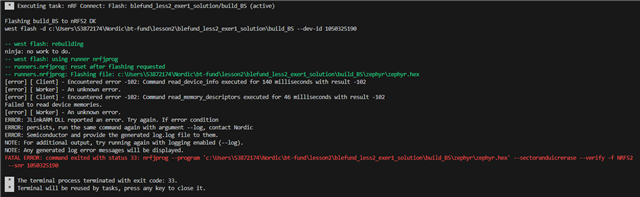
I am getting an error when attempting to access the memory of my device.
I've uploaded a picture of the printed error.
I've also tried using the quick start app to upload the hello world example in the NRF desktop and am having the same issue. I've uploaded the associated logfile.
Are there any areas you'd reccomend looking into?
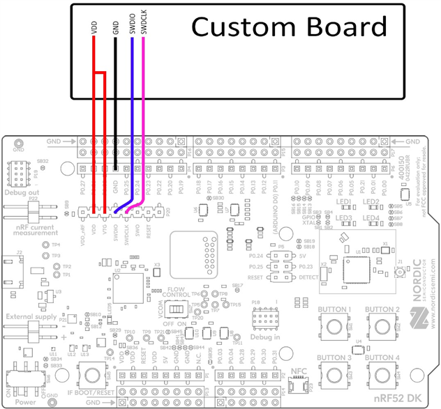
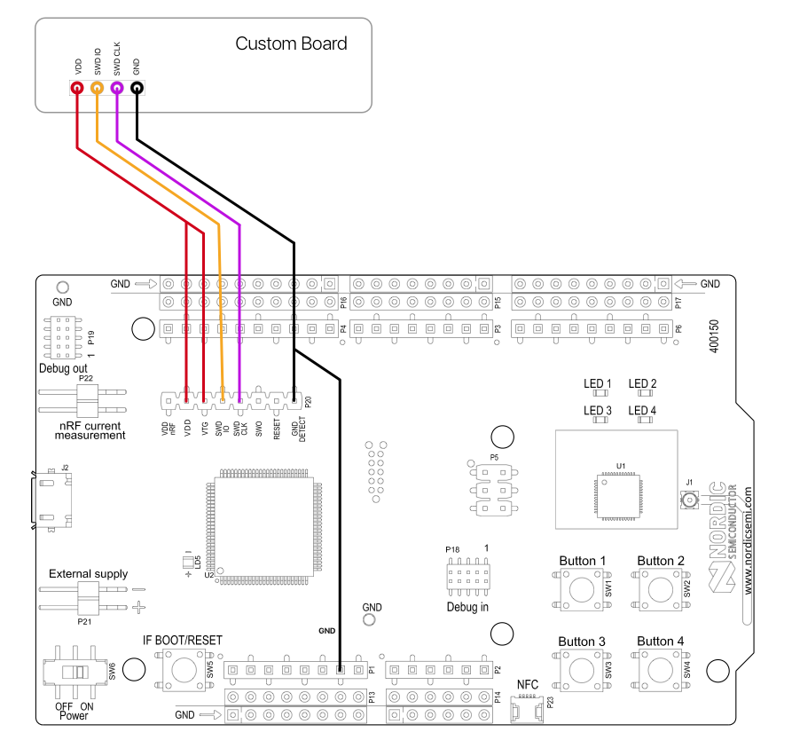
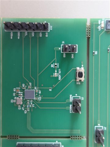
I've gone over the board and all connections seem to be stable.
2025-09-02T00:14:28.615Z INFO Initialising the bundled nrfutil device
2025-09-02T00:14:28.647Z DEBUG Started watching devices
2025-09-02T00:14:32.202Z INFO Using the bundled core version for nrfutil device: 8.1.1
2025-09-02T00:14:32.418Z INFO Using nrfutil-device version: 2.10.2
2025-09-02T00:14:32.418Z INFO Using nrf-device-lib version: 0.17.71
2025-09-02T00:14:32.419Z INFO Using nrf-probe version: 0.38.0
2025-09-02T00:14:32.419Z INFO Using JLink version: JLink_V8.22
2025-09-02T00:14:32.420Z INFO Your version of SEGGER J-Link (8.22) is newer than the one this app was tested with (8.18). The tested version is not required, and your J-Link version will most likely work fine. If you get issues related to J-Link with your devices, use the tested version.
2025-09-02T00:14:34.025Z DEBUG Selected device: nRF52 DK
2025-09-02T00:14:34.086Z DEBUG Changed step: Info
2025-09-02T00:14:42.696Z DEBUG Changed step: Rename
2025-09-02T00:14:45.062Z DEBUG Changed step: Program
2025-09-02T00:16:04.301Z DEBUG Changed step: Verify
2025-09-02T00:16:07.311Z INFO Opened port with options: {"path":"COM14","baudRate":115200}
2025-09-02T00:16:08.415Z ERROR Failed with exit code 1.
One or more reset tasks failed:
 * 1050325190: Device error: Failed to write DebugPort register 0x08: Unknown Error in J-Link DLL (error code =-1) (Generic).
Message: Failed to reset 1050325190, Device error: Failed to write DebugPort register 0x08: Unknown Error in J-Link DLL (error code =-1).
2025-09-02T00:16:08.430Z INFO Closed port: COM14
2025-09-02T00:16:11.424Z DEBUG Changed step: Program