Need Help Verifying BLE Antenna Matching Circuit on nRF52810 Custom Board

Hi Everyone,

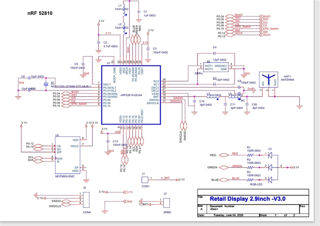
We are developing a custom retail display solution based on the nRF52810 SoC.

Currently, we are facing an issue where BLE advertising does not start properly on our board.

We suspect that the antenna matching circuit might have a problem.

I am attaching our circuit diagram showing the antenna matching network, which includes:

  • C11 and C12 = 12 pF

  • L3 and L4 = 3.9 nH

  • C26 = 0.8 pF

The operating frequency is 2.45 GHz (BLE band) and the target input impedance is 50 Ω.

Could you please help review the antenna matching section and confirm if the design looks correct?
If there are any improvements or corrections you suggest, that would be extremely helpful.

5238.nRF epaper pcbAnt.rar

2677.Epaper 2.9 V2.0 Smd Ant.rar

Thanks in advance!

M. Praveen

Parents Reply Children
  • M.Praveen said:
    We did not calculate and design the antenna ourselves; instead, we based the design on the dimensions of the antenna from another sample

    That is perfectly fine, as long as the design is followed it should work ok, and with a few extra matching components it can be tuned if needed. 


    M.Praveen said:
    I have attached the datasheet of the chip antenna for your reference.

    For the 2450AT18A100 antenn it is important for follow the recommendations and looks like that has been done. It is possible to ask johansontechnology for help as well as they do have support. 


    Values look ok\realistic but it is impossible to accurately give feedback on what component values are best without physically testing the device either conducted or radiated. 

    So far all looks ok and is a good starting point but it is likely that the two versions need different values. 

    Regards,
    Jonathan

Related