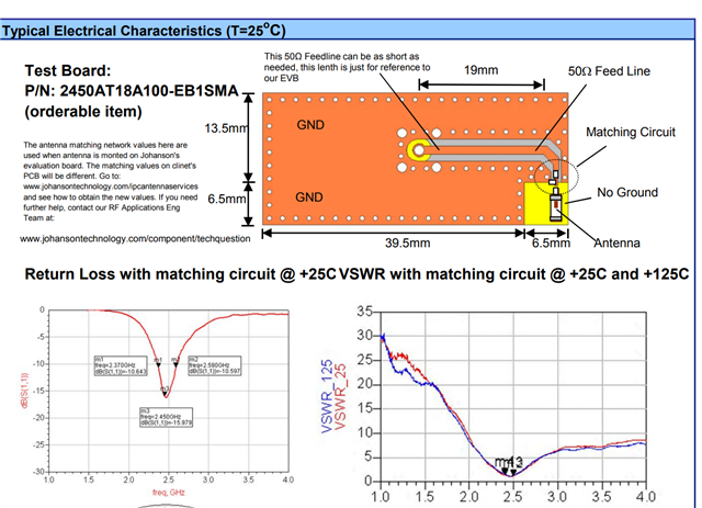
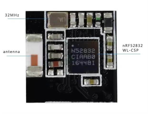
PCB Review

Hello,

I am attempting to develop an open source nRF52832 PCB design, aiming to minimize the footprint as much as possible.

Thus, I attempted to cramp as many components in a tight space as possible.

I know that my design, deviating from the reference PCB, probably sacrifices quite a bit of RF quality and signal strength.

Yet, I wanted to ask Nordics opinion on this design, and what I could improve.

Thanks a lot!nrf52_micro.zip

Parents
  • We will happily have a look at this and do our best to help you reach you goal here

    probably sacrifices quite a bit of RF quality and signal strength.

    You made a very compact design here so RF performance will likely suffer. I see that you are using a chip antenna, can you link to the antenna of choice? 

    Most Nordic products have their own radio matching network, and the antennas often have their own as well so usually you would need to add the recommended components for the antenna of choice. 

    See https://devzone.nordicsemi.com/guides/hardware-design-test-and-measuring/b/nrf5x/posts/general-pcb-design-guidelines-for-nrf52-series for some more details on what we recommend. 

    https://devzone.nordicsemi.com/guides/hardware-design-test-and-measuring/b/nrf5x/posts/nrf52832-specific-pcb-guidelines 

    Also maybe have a look at our nRF52805 CSP variant, its small. https://devzone.nordicsemi.com/guides/hardware-design-test-and-measuring/b/nrf5x/posts/nrf52805-specific-pcb-guidelines , here it also shows the LDO setup https://docs.nordicsemi.com/bundle/ps_nrf52805/page/ref_circuitry.html#ariaid-title5 

    If you want the area even smaller you can mount some of the components like the crystal on the bottom layer. 

    What is the goal here in terms of RF performance? 


    Also, you do not have access to the programming pins here, SWDIO and SWDCLK, unless the SoC comes pre-programmed this will be difficult to work with. 

    Regards,
    Jonathan

  • Thanks a lot, I really appreciate the feedback!

    1. I have linked the datasheets of all components in the kicad schematic, if I am not mistaken. Could you please check there? If I recall correctly, I was intending to use 2450AT18A100, which should be pre-tuned to 50 ohms.

    2. I could mount components on the bottom, but would that not make the whole module unmountable?

    3. This board is just a prototype, and I have no specific RF goals in mind. I just need a few meters of connection. Could you give me some sort of scale on what to expect here, given the provided chip antenna?

    4. Oh, I must have missed the debug pins. My bad...

    Again, thanks a lot! For a first attempt of designing something like this, it is really overwhelming. Help like this really helps to understand a lot of things!

  • Daniel Dakhno said:
    1. I have linked the datasheets of all components in the kicad schematic, if I am not mistaken. Could you please check there? If I recall correctly, I was intending to use 2450AT18A100, which should be pre-tuned to 50 ohms.

    Did not see the antenna, might have missed this. But the 2450AT18A100 is a antenna we see a lot so good place to start. But the antenna still needs some components to be matched properly, the exact components will differ from design to design. 


    Also if you see in the datasheet here you see that the board used for measuring the results here is a lot larger then the design you are making. These chip antennas will perform different to some degree depending on how much or how large of a continues GND plane it has. 
    A small ground plane for these chip antennas often result in a narrower band, so iif the antenna is de-tuned it can perform a lot worse. 


    Daniel Dakhno said:
    2. I could mount components on the bottom, but would that not make the whole module unmountable?

    Directly on a flat surface it would be hard to mount it, but you can place it on the edge of the mother PCB, like what is done with most modules, or have a cutout for where the components are. This does make things more complex but it is possible. 


    Daniel Dakhno said:
    . This board is just a prototype, and I have no specific RF goals in mind. I just need a few meters of connection. Could you give me some sort of scale on what to expect here, given the provided chip antenna?

    It will depend, but at its current setup I would not expect good performance, but it should work. would expect maybe up to a meter in distance, if lucky more. It could be that it gives you 3+ meters, but I would not expect that. 


    Happy to help here, so feel free to ask and I will do my best to explain

    Regards,
    Jonathan

  • Hello,

    thanks again.

    I am looking at a HolyIOT 17095 module, and they seemed to have the same ideas I had.

    As far as I can see, they are also not using more components than I do, yet I had amazing performance (10+ meters) with those modules.

    1. Do you have an Idea how they achieve that performance?

    2. You mentioned that I have not connected the debug pins. While that is true from the schematic, could you please also confirm that from the PCB design? I have connected most gpios only in the PCB. Is there a better way to do this?

    Kind regards,

    Daniel

  • Hello again,

    I am seeing this ticket being passed around, as it seems.

    Is there anything further required from me?

    Cheers!

  • Hi an happy new year!

    Ticket has been passed around as there has been few people working during this holiday, so things move a round a bit while the ones left working are keeping track of everything. 


    Daniel Dakhno said:
    As far as I can see, they are also not using more components than I do, yet I had amazing performance (10+ meters) with those modules.

    That is impressive. I have not looked at the HolyIOT module so not sure how well it performs, could be that the device has decent performance, but it is difficult for us to know and also difficult to give the "Ok this is fine" as we have seen many designs similar that preform relay bad.  Also some antennas are more forgiving then others.


    Daniel Dakhno said:
    2. You mentioned that I have not connected the debug pins. While that is true from the schematic, could you please also confirm that from the PCB design?

    G1 and F1 is not connected so no SWD pins, this will make it difficult to program. At least I don't see the pins connected to anything external. But I did not download the files again, only checked the one I already had. 


    Daniel Dakhno said:
    I have connected most gpios only in the PCB. Is there a better way to do this?

    On such tiny designed you just have to find a place to route them, there is always a compromise, and keeping the layer count low does not make it easier.  The proper way to do it would be to use some in pad vias that can route out the pins on the bottom layer.

    Regards,
    Jonathan

Reply
  • Hi an happy new year!

    Ticket has been passed around as there has been few people working during this holiday, so things move a round a bit while the ones left working are keeping track of everything. 


    Daniel Dakhno said:
    As far as I can see, they are also not using more components than I do, yet I had amazing performance (10+ meters) with those modules.

    That is impressive. I have not looked at the HolyIOT module so not sure how well it performs, could be that the device has decent performance, but it is difficult for us to know and also difficult to give the "Ok this is fine" as we have seen many designs similar that preform relay bad.  Also some antennas are more forgiving then others.


    Daniel Dakhno said:
    2. You mentioned that I have not connected the debug pins. While that is true from the schematic, could you please also confirm that from the PCB design?

    G1 and F1 is not connected so no SWD pins, this will make it difficult to program. At least I don't see the pins connected to anything external. But I did not download the files again, only checked the one I already had. 


    Daniel Dakhno said:
    I have connected most gpios only in the PCB. Is there a better way to do this?

    On such tiny designed you just have to find a place to route them, there is always a compromise, and keeping the layer count low does not make it easier.  The proper way to do it would be to use some in pad vias that can route out the pins on the bottom layer.

    Regards,
    Jonathan

Children
Related