Unable to flash custom nRF52840 board using nRF52840dk - Device error: Setting the debug port SELECT register failed while powering up sys and debug regions (Unknown error in the J-Link DLL (error code =-1)).

I am using nRF Connect SDK 3.2.1 and Toolchain 3.2.1. The hardware I am using is the nRF52840DK and a custom board with the Raytac MDBT50Q-P1MV2 - which contains the nRF52840. I created a custom board in the SDK and built a program that blinks an onboard LED on the custom board. The program builds without error, but when I try to flash the code to the custom board I get the following error - Device error: Setting the debug port SELECT register failed while powering up sys and debug regions (Unknown error in the J-Link DLL (error code =-1)). I saw a similar question 4 months ago, but no solution was ever obtained (or if it was the developer never replied). My custom board is powered by a 3.3V LDO regulator that is powered by a 3.8V power supply. The SWD setup uses a 10 pin connector with with pinout: 1: VCC= 3.3V supplied from LDO regulator, 2: SWDIO, 3: GND, 4: SWCLK, 5: GND, 6:SWO, 7: GND, 8: N/C, 9: GND. 10: nRESET. I use a ribbon cable with connectors purchased from Adafruit for the J-Link edu mini to connect my board to the DK Debug Out port P19. When I power my board and connect it to the DK, I see the following voltages on some pins I can access: On SCL and SDA pins I see 2.3V; On SDIO I see 3V. On SWCLK I see 0V. (One odd thing is if I power my board and do not connect it to the DK, I see a 1.6V, 260uS pulse every 34mS on the SWDIO line - so about 30Hz)

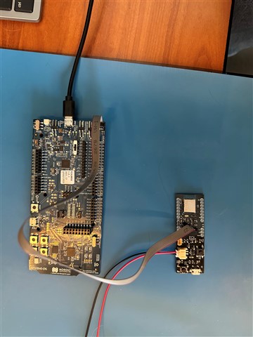
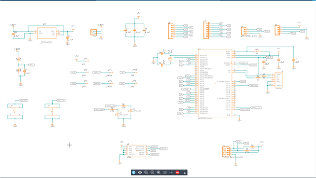
I designed the board (based on the Adafruit nRF52840 feather and assembled it myself. This is the first time I've used the Raytac module, so I don't know exactly how to prove it is working correctly before flashing it. I have attached a picture of the flashing setup - my board and the SDK with ribbon connector, and a picture of my schematic for reference. Here is the text from the Output and Terminal windows in nRF Connect extension for VS Code: 

Output
[13:47:34] build --build-dir c:/myfw/protoboard/button/build --domain button
[13:47:36] Success.
[13:47:40] flash -d c:\myfw\protoboard\button\build --domain button --dev-id 1050257059
[13:47:42] Failure (code 1).


Terminal

 *  Executing task: nRF Connect: Build [incremental]: button/build/button

Building button
west build --build-dir c:/myfw/protoboard/button/build --domain button
-- west build: building domain(s): button
ninja: no work to do.
 *  Terminal will be reused by tasks, press any key to close it.

 *  Executing task: nRF Connect: Flash: button/build/button

Flashing button to nRF52840 DK
west flash -d c:\myfw\protoboard\button\build --domain button --dev-id 1050257059
-- west flash: rebuilding
[0/5] Performing build step for 'button'
ninja: no work to do.
[4/5] cmd.exe /C "cd /D C:\myfw\protoboard\button\build\_sysbuild && C:\ncs\toolchains\66cdf9b75e\opt\bin\cmake.exe -E true"
-- west flash: using runner nrfutil
-- runners.nrfutil: reset after flashing requested
-- runners.nrfutil: Flashing file: C:\myfw\protoboard\button\build\merged.hex
-- runners.nrfutil: Connecting to probe
Error: One or more batch tasks failed:
 * 1050257059: Device error: Setting the debug port SELECT register failed while powering up sys and debug regions (Unknown Error in J-Link DLL (error code =-1)).
   
   This might indicate that the debug port is unavailable. Please double-check device power sFATAL ERROR: command exited with status 1: nrfutil --json device x-execute-batch --batch-path 'C:\myfw\protoboard\button\build\button\zephyr\generated_nrfutil_batch.json' --serial-number 1050257059

 *  The terminal process terminated with exit code: 1.
 *  Terminal will be reused by tasks, press any key to close it. 

Appreciate your expert review and advice,

Lonnie

Parents
  • Hi

    The behavior here definitely sounds like a hardware issue since neither the DK or the J-Link is able to connect to it.

    I asked one of my colleagues with more HW expertise than me. There is nothing obviously wrong, but for possible future revisions, you can improve the grounding in general on your board.

    One thing to note though is that you run the J-Link on full speed. During connection issues like this you can try to lower the J-Link speed to see if that lets you connect and program the boards.

    You can also, just to try connect the 10 pin cable 180 degrees the other way in case that is the issue (a common one if the header isn't supported with plastic to show which way it should be connected).

    Best regards,

    Simon

  • Simon, 

    First, thank you for your expert advise and guidance. I would like to ask once more for your help as I think I uncovered something significant, and I believe a Nordic expert is needed to answer my question. 

    Bottom line - I believe my custom board is pulling down the output voltage of the SWDIO and SWCLK lines of the DK or J-Link)

    In order to confirm the signaling is correct between the DK (or J-Link) and my custom board I connected only the necessary signal lines (SWDIO, SWCLK, GND and SWO_SEL) using breakout boards and jumpers. The DK and the J-Link both continued to give the same errors (they cannot connect to the custom board). I then attached my oscilloscope and logic analyzer to the lines. The O-scope showed data and clock on the respective lines, but the voltage shown was only 2.23V. My logic analyzer was able to decode the data and clock even with this reduced voltage and I have attached a couple of screen shots of that data (I looked for SWD protocol info for Nordic and J-Link to understand what was sent but I have not been able to locate that info yet - perhaps you can analyze the signals and tell if there is comms between the custom board and DK - or if the data is only that which the DK sends out - with no response. This is my hunch). I then removed the SWDIO and SWCLK signals from the custom board and connected them only to the o-scope. I then tried to connect the JLink probe to the custom board. The o-scope showed SWDIO data at 3.1V. So it appears that the custom board is pulling the signal lines low enough (2.3V vs 3.1V) that they are below the voltage threshold for a "1". 

    Going back to my previous note, could the fact that VDDH is floating, and not tied to VDD cause this? If not what else could cause this phenomenon? On my PCB, SWDIO and SWCLK are point to point from the RAYTAC module to the connector (and a test point) - so nothing else could be pulling them low. 

    Thanks for your help,

    Lonnie

Reply
  • Simon, 

    First, thank you for your expert advise and guidance. I would like to ask once more for your help as I think I uncovered something significant, and I believe a Nordic expert is needed to answer my question. 

    Bottom line - I believe my custom board is pulling down the output voltage of the SWDIO and SWCLK lines of the DK or J-Link)

    In order to confirm the signaling is correct between the DK (or J-Link) and my custom board I connected only the necessary signal lines (SWDIO, SWCLK, GND and SWO_SEL) using breakout boards and jumpers. The DK and the J-Link both continued to give the same errors (they cannot connect to the custom board). I then attached my oscilloscope and logic analyzer to the lines. The O-scope showed data and clock on the respective lines, but the voltage shown was only 2.23V. My logic analyzer was able to decode the data and clock even with this reduced voltage and I have attached a couple of screen shots of that data (I looked for SWD protocol info for Nordic and J-Link to understand what was sent but I have not been able to locate that info yet - perhaps you can analyze the signals and tell if there is comms between the custom board and DK - or if the data is only that which the DK sends out - with no response. This is my hunch). I then removed the SWDIO and SWCLK signals from the custom board and connected them only to the o-scope. I then tried to connect the JLink probe to the custom board. The o-scope showed SWDIO data at 3.1V. So it appears that the custom board is pulling the signal lines low enough (2.3V vs 3.1V) that they are below the voltage threshold for a "1". 

    Going back to my previous note, could the fact that VDDH is floating, and not tied to VDD cause this? If not what else could cause this phenomenon? On my PCB, SWDIO and SWCLK are point to point from the RAYTAC module to the connector (and a test point) - so nothing else could be pulling them low. 

    Thanks for your help,

    Lonnie

Children
No Data
Related