Good day,
We are developing a board with a nRF54L15 + nRF7002 for BLE and WiFi connectivity.
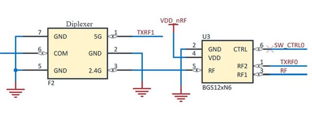
The Nordic nRF54L15 + nRF7002 reference design has been a good starting point. It demonstrates the use of a single antenna for WiFi and BLE, using a BGS12SN6 RF switch to connect either RF input to the antenna.
The downside of the RF switch is that it introduces a quiescent current of 63 uA (typ, datasheet) at all times when powered on. The reference design connects the RF switch directly to the main power supply.
What is the recommended approach to reduce power consumption of the RF switch when not in use? Can VDD be controlled by the MPSL CX/FEM API and are there any examples for this?
Note: This ticket looks related: Quiescent current - Thingy:91X vs. Thingy:91 with BLE enabled , however the conclusion is that:
This switch is used to select whether the 2.4 GHz antenna is used for Wi-Fi or BLE. When BLE is enabled in the connectivity bridge, the switch is continuously powered, since the time to turn on the load switch U5, which in turn powers the RF switch, is too long (hundreds of µs) to toggle it dynamically using the BLE stack.
This would appear to contradict the datasheet for the BGS12WN6 - The typ. power up setting time is 5.8 us, well below the 40 us TX_RAMP_UP_TIME described as the maximum allowable for dynamic control of RF FEM: https://docs.nordicsemi.com/bundle/ncs-2.6.4/page/nrf/device_guides/working_with_fem.html
Looking forward to your feedback.
Dom