Hi,
We are working on a custom design for IoT cellular communication (NB-IoT), using the nRF9151. We've done some testing with the SMA DK, and are at the stage of PCB design. This is replacing an existing solution with a different manufacturer cellular modem and it integrates with other features, so there are some constrains and thus some questions have come up during design, if you could help us:
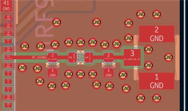
- Regarding the LTE antenna, currently we use a passive LTE antenna by The Antenna Company, which is located off-board, attached to the IoT device's enclosure interior and connects to the PCB via a few cm long U.FL connector. With the old modem we're using only one Pi network for matching (we'll be using the TAC matching service), with the nRF PCB design so far, this essentially constitutes almost the entire RF trace length from the nRF pin to the U.FL connector using 0402 components, so it's a short trace about 7 mm (50 ohm). I see this isn't quite the configuration on the non-SMA DK schematic which has two Pi's, do you think it will be enough in our application to include just the one Pi-network for matching the external antenna?
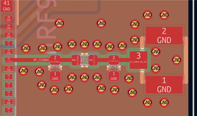
- Concerning this point on the ANT pin's documentation: "Avoid excessive capacitance in routing by opening ground layers under component pads. For example, if the routing is on the top PCB layer, open the ground plane under the ANT pad on the next metal layer." So our stackup is JLC's 7628 FR4, with 4 layers and 1.6 mm board, the RF on top and reference on the layer 2 ground plane for coplanar single-ended. Do I understand correctly that for this setup, this would refer to a copper exclusion area in the layer 2 copper plane under the nRF ANT pin and the connector's pad, even though it is the reference? Would layers 3 and 4 be included in this exclusion also? I noticed the DK appears to use layer 3 as the reference and leaves layer 2 open, which isn't our case. And if this suggestion applies to our case, would it be more optimal to extend the exclusion a bit larger than the pad area, or stick to strictly the pad area?
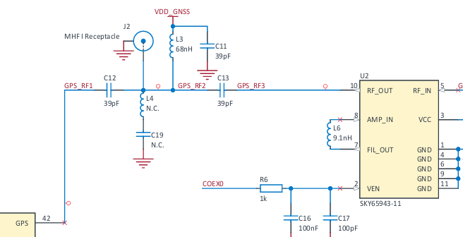
- We'll be integrating the nRF's GNSS capabilities into the device as well, our current GNSS antenna is passive, with similar mounting and connection as the cellular antenna, so a front-end module is necessary, we'll be using the SKY65943-11 from the non-SMA DK. I see that the DK includes a bias network with L3, C11, C12 and C13, however I've also found a different reference design and answer here in the Devzone that this is for using an active antenna. However, the non-SMA DK schematic still includes this together with the front-end, even though the Taoglas antenna included seems to be passive. Can you confirm that for a passive external GNSS antenna and using the SKY, we could omit this bias network and connect RF_OUT straight to the nRF GNSS IN?
- More on the application side, the intent is to use some modification of the Serial Modem application. The host is an off-board ESP32 with UART communication, however owing to the existing overall design, there are no more IO's available on the ESP for hardware flow control or UART power management, so TX and RX are the only available signals. I understand from nRF documentation and other questions here that we can modify the serial modem app to disable flow control and not configure RTS and CTS on GPIOs. I see reference to also not using power management, but it's ambiguous to me how DTR should be handled, as the serial modem documentation states it should still be pulled active [low] when power management is not used. To be clear, is not using UART power management for serial modem a configuration step whereby no DTR is configured on any GPIO and irrelevant to UART TX/RX use, or should this signal always be configured to some GPIO and not using power management equates to permanently driving said pin active-low? We have plenty of GPIOs available nRF-side as only UART TX/RX and a couple status LED drivers are needed, just need to know if we should include extra circuitry to drive DTR active-low at all times or can leave all remaining GPIOs floating.
Thanks in advance.
Best regards,
Diogo