How to fix the voltage mismatch between VTref and VDD on the target board?

Hi everyone. I’m currently working on a custom board based on the nRF5340, but I’m unable to connect to the board when trying to flash it via the SWD interface using J-Link. Here is the error message from my SDK:
Error: One or more device info tasks failed:
302005664: Device error: A timeout occurred while handling debug power: Timed out trying to power sys and debug region
(Generic)
When troubleshooting with J-Link Commander, I got the following output:
J-Link>st
VTref=1.673V
ITarget=0mA
TCK=1 TDI=0 TDO=0 TMS=0 TRES=1 TRST=?
Supported target interface speeds:
  • 96 MHz/n, (n>=24). => 4000kHz, 3840kHz, 3692kHz, ...
However, I measured 3.1V on the SWD VDD pin with a multimeter, and the main chip power supply seems normal.
Also, because I cannot connect, I cannot try the nrfjprog --recover command suggested by AI.
Does anyone have any good solutions?
Parents
  • Hello,

    ''

    • Is the VTref value reported by JLinkExe measured directly from the VTref pin on the target, or can it reflect an internal voltage on the DK under some conditions?
    • If VTref is incorrectly detected as 3.3 V, could the SWD signals be driven at 3.3 V?''

    There is no built-in level shifter for the on-board debugger so it will not adjust the Input-output (IO) voltage based on the Vterf voltage. The IO voltage of the DK must match the IO voltage on the target for this reason what I mentioned in the previous reply also.

    To power the 1.8V custom board from nRF5340 DK, you can follow the steps mentioned below:

    1. Connect a USB to both J2 and J3 (nRF USB port)

    2. On the SW9, switch from ''VDD'' to ''USB''

    3. Power up the DK

    Then you can get 1.8V from the debugger.

    Thanks.

    BR
    Kazi

  • Hello Kazi,

    I am a colleague of João working on the same board. I would like to clarify a few things.

    There seems to be some conflicting information about the purpose of the SB19 and the ability of the nRF5340 DK to drop the VDD level to 1.8 V based on the VIO_REF level supplied by an external board.

    The nRF5340 DK User Guide does not mention this, and some answers here on DevZone suggest it's not possible. However, some answers suggest it is possible. More specifically, in https://devzone.nordicsemi.com/f/nordic-q-a/115349/programming-external-mcu-with-nrf5340-dk this is clearly stated as being possible, while in https://devzone.nordicsemi.com/f/nordic-q-a/104739/i-can-t-program-external-board-with-nrf5340-2-0-2/450783 it is even acknowledged that this information is missing from the DK User Guide.

    We have tested and confirmed this behavior a few months ago, and have been using the DK this way to program and debug our custom boards since then.

    As João stated, some of our boards have presented some issues related to this IC he described, which has a maximum supply voltage of 1.98 V. We are not using the DK to supply power to our custom board. It is being powered separately. Our question is if this behavior of dropping VDD based on VIO_REF (which we confirmed to be true) could have some sort of delay and, therefore, could briefly expose this IC to a voltage over its limit.

    Thanks.

    Felipe.

  • Hello Felipe,

    The DK will drive the SWD pins to the VDD level of DK for 100% of the time. The Vtref is only used to see if there is voltage on the external board, it does not impact the SWD pin voltage whatsoever.

    You must ensure that the voltage on the external board is exactly the same as the DK. Failing to do so can cause damage to the external board or to the DK.

    It needs to be ensured also that no hot swapping of external boards as that may also damage the DK or the external target.

    This is the case for all nRF52/53 kits. The nRF54 kits have different limitations, which is described in the HW user guides.

    Thanks.

    BR

    Kazi

  • Dear Kazi, dear all,

    As I said earlier, the VTref voltage senses the target's 1.8 V supply. Unlike what was stated in your last comment, however, with SB19 shorted the nRF5340 DK does adjust its I/O voltage to the target VDD level, allowing debugging of externally powered targets operating at different supply voltages.

    My main concern was whether, during this adjustment, any transient voltage could briefly drive the target above 1.98 V, which is the absolute maximum supply voltage of the IC that failed on our prototypes. I also wanted to verify whether connecting the debugger or resetting the target could generate any voltage transient on the power rail or on the SWD signals.

    I have two faulty prototype boards in which I removed the shorted IC to allow further investigation. One board still contains the PMIC and is powered through a 4 V supply connected to VBAT. The second board no longer has the PMIC and is powered directly from a laboratory supply at 1.88 V on VDD.

    I performed the following oscilloscope measurements. Each measurement was done more than once to ensure consistency.

    Board without PMIC (VDD supplied directly at 1.88 V)

    Test 1.1
    Board connected to the DK through SWD, external supply initially OFF. Trigger set at 1.8 V on VDD. The board was then powered with 1.88 V.

    Result: VDD rises smoothly to 1.88 V with no overshoot or transient.

    Test 1.2
    Same setup as above, but with the board already powered. Trigger set at 1.8 V on VDD while removing power.

    Result: no trigger event. No transient observed during power-down.

    Test 1.3
    Board powered at 1.88 V. Trigger set at 1 V on SWCLK. A SWD connection was initiated using J-Link Commander (JLinkExe, than connect, than S for SWD).

    Result: SWCLK pulses are generated, but their amplitude remains below 1.8 V.

    Test 1.4
    Board powered at 1.88 V. Trigger set at 1 V on SWDIO. A SWD connection was initiated.

    Result: SWDIO pulses reach approximately 1.86 V.

    Test 1.5
    Board powered at 1.88 V. Trigger set on the TRACE/SWO pin.

    Result: no activity observed. The TRACE/SWO line is not driven during SWD connection.

    Test 1.6
    Board powered at 1.88 V but disconnected from the DK. Trigger set at 1.88 V on VDD. The SWD cable was then connected.

    Result: connecting the debugger does not produce any overshoot or disturbance on VDD.

    Board with PMIC (powered from 4 V applied to VBAT)

    Test 2.1
    Board connected through SWD. External supply initially OFF. Trigger set at 1.8 V on VDD. VBAT was then powered with 4 V.

    Result: VDD rises smoothly to approximately 1.8 V with no overshoot.

    Test 2.2
    Board powered from VBAT. Trigger set at 1.8 V on VDD while removing power.

    Result: no trigger event. No transient observed.

    Test 2.3
    Board powered from VBAT. Trigger set at 1 V on SWCLK. A SWD connection was initiated.

    Result: SWCLK pulses remain below 1.8 V.

    Test 2.4
    Board powered from VBAT. Trigger set at 1 V on SWDIO.

    Result: SWDIO reaches approximately 1.8 V.

    Test 2.5
    Board powered from VBAT. Trigger set on TRACE/SWO.

    Result: no activity observed.

    Test 2.6
    Board powered from VBAT and disconnected from the debugger. Trigger set at 1.8 V on VDD. The SWD cable was connected.

    Result: no overshoot or disturbance on the VDD rail.

    Test 2.7
    Board powered from VBAT and disconnected from the debugger. Trigger set at 1 V on SWCLK. The SWD cable was connected.

    Result: no overshoot observed. SWCLK always remains below 1.8 V.

    Test 2.8
    Board powered from VBAT and disconnected from the debugger. Trigger set at 1 V on SWDIO. The SWD cable was connected.

    Result: no overshoot observed. SWDIO rises smoothly to approximately 1.8 V.

    Additional measurements on the debugger
    Test 3.1
    The RESET signal on the DK was monitored while connecting the SWD cable.

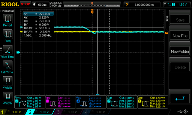
    Result: RESET transitions from approximately 3 V to 1.8 V, with an intermediate point of 2V3, depending on how the connector mates mechanically. Temporary overshoots approaching 3 V can occasionally be observed on the DK side. I couldn't measure in the target side due to the physical placement of the connector.

    However, these events are not reflected on the target VDD or SWD signals. Picture bellow shows the transition between the 2V3 midpoint to 1V8 of the target.

    Test 3.2
    VTref on the DK was monitored while connecting the SWD cable.

    Result: VTref transitions rapidly from 0 V to 1.8 V with no overshoot observed, even when the connector is intentionally mated slowly.

    Test 3.3
    Signals on the DK connector were monitored during cable insertion.

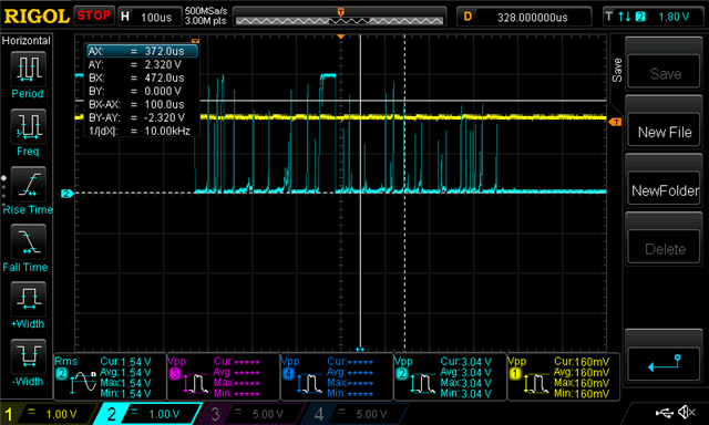
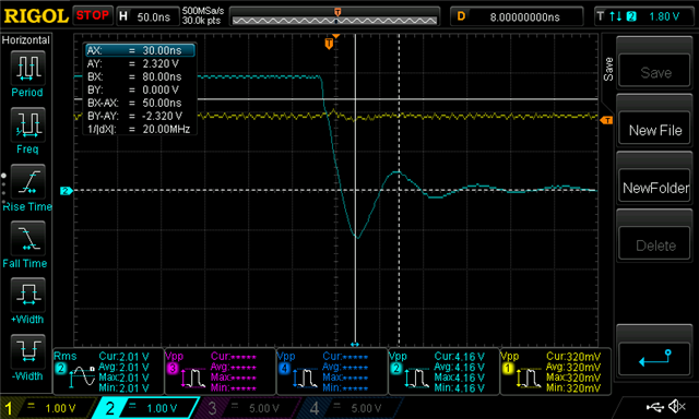
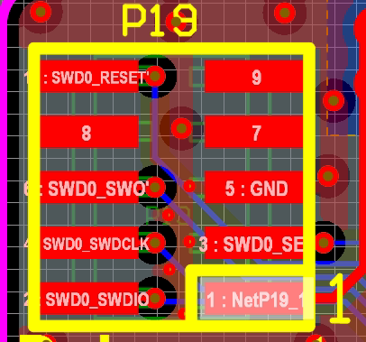
    Result: Here I found that the output debugger of the DK doesn't follow the standard Segger pinout as we did in the prototype. I checked this inconsistency when measured 3 V in pin 3 of the connector, which was supposed to be GND in the standard connection. I checked the HW files and saw that this is SWD0_SEL in the DK.

    When connecting the SWD, the SWD0_SEL signal is grounded through the target, and may ring or glitch a bit before doing so. This could possibly lead to strange behavior, but I am still skeptical it explains the dead IC. Here two pictures of the voltage in pin 3:

    Conclusions
    Based on these measurements, I have not been able to reproduce any condition in which the nRF5340 DK drives either the target VDD rail or the SWD interface above the target operating voltage. All observed SWD signals remained at or below the target VDD, and connecting the debugger did not produce any measurable overshoot on the target power rail, even when intentionally making lets say a noisy connection. 

    I could see a strange behavior on the RESET pin and on pin 3 of the connector, nevertheless I do not believe they can explain what we have (do you?).

    If there is another failure mechanism that you believe could explain these observations, I would greatly appreciate your suggestions, as I would like to investigate it further.

    For reference, the DK's connector:

    And ours:

    []'s
    João Colombari

Reply
  • Dear Kazi, dear all,

    As I said earlier, the VTref voltage senses the target's 1.8 V supply. Unlike what was stated in your last comment, however, with SB19 shorted the nRF5340 DK does adjust its I/O voltage to the target VDD level, allowing debugging of externally powered targets operating at different supply voltages.

    My main concern was whether, during this adjustment, any transient voltage could briefly drive the target above 1.98 V, which is the absolute maximum supply voltage of the IC that failed on our prototypes. I also wanted to verify whether connecting the debugger or resetting the target could generate any voltage transient on the power rail or on the SWD signals.

    I have two faulty prototype boards in which I removed the shorted IC to allow further investigation. One board still contains the PMIC and is powered through a 4 V supply connected to VBAT. The second board no longer has the PMIC and is powered directly from a laboratory supply at 1.88 V on VDD.

    I performed the following oscilloscope measurements. Each measurement was done more than once to ensure consistency.

    Board without PMIC (VDD supplied directly at 1.88 V)

    Test 1.1
    Board connected to the DK through SWD, external supply initially OFF. Trigger set at 1.8 V on VDD. The board was then powered with 1.88 V.

    Result: VDD rises smoothly to 1.88 V with no overshoot or transient.

    Test 1.2
    Same setup as above, but with the board already powered. Trigger set at 1.8 V on VDD while removing power.

    Result: no trigger event. No transient observed during power-down.

    Test 1.3
    Board powered at 1.88 V. Trigger set at 1 V on SWCLK. A SWD connection was initiated using J-Link Commander (JLinkExe, than connect, than S for SWD).

    Result: SWCLK pulses are generated, but their amplitude remains below 1.8 V.

    Test 1.4
    Board powered at 1.88 V. Trigger set at 1 V on SWDIO. A SWD connection was initiated.

    Result: SWDIO pulses reach approximately 1.86 V.

    Test 1.5
    Board powered at 1.88 V. Trigger set on the TRACE/SWO pin.

    Result: no activity observed. The TRACE/SWO line is not driven during SWD connection.

    Test 1.6
    Board powered at 1.88 V but disconnected from the DK. Trigger set at 1.88 V on VDD. The SWD cable was then connected.

    Result: connecting the debugger does not produce any overshoot or disturbance on VDD.

    Board with PMIC (powered from 4 V applied to VBAT)

    Test 2.1
    Board connected through SWD. External supply initially OFF. Trigger set at 1.8 V on VDD. VBAT was then powered with 4 V.

    Result: VDD rises smoothly to approximately 1.8 V with no overshoot.

    Test 2.2
    Board powered from VBAT. Trigger set at 1.8 V on VDD while removing power.

    Result: no trigger event. No transient observed.

    Test 2.3
    Board powered from VBAT. Trigger set at 1 V on SWCLK. A SWD connection was initiated.

    Result: SWCLK pulses remain below 1.8 V.

    Test 2.4
    Board powered from VBAT. Trigger set at 1 V on SWDIO.

    Result: SWDIO reaches approximately 1.8 V.

    Test 2.5
    Board powered from VBAT. Trigger set on TRACE/SWO.

    Result: no activity observed.

    Test 2.6
    Board powered from VBAT and disconnected from the debugger. Trigger set at 1.8 V on VDD. The SWD cable was connected.

    Result: no overshoot or disturbance on the VDD rail.

    Test 2.7
    Board powered from VBAT and disconnected from the debugger. Trigger set at 1 V on SWCLK. The SWD cable was connected.

    Result: no overshoot observed. SWCLK always remains below 1.8 V.

    Test 2.8
    Board powered from VBAT and disconnected from the debugger. Trigger set at 1 V on SWDIO. The SWD cable was connected.

    Result: no overshoot observed. SWDIO rises smoothly to approximately 1.8 V.

    Additional measurements on the debugger
    Test 3.1
    The RESET signal on the DK was monitored while connecting the SWD cable.

    Result: RESET transitions from approximately 3 V to 1.8 V, with an intermediate point of 2V3, depending on how the connector mates mechanically. Temporary overshoots approaching 3 V can occasionally be observed on the DK side. I couldn't measure in the target side due to the physical placement of the connector.

    However, these events are not reflected on the target VDD or SWD signals. Picture bellow shows the transition between the 2V3 midpoint to 1V8 of the target.

    Test 3.2
    VTref on the DK was monitored while connecting the SWD cable.

    Result: VTref transitions rapidly from 0 V to 1.8 V with no overshoot observed, even when the connector is intentionally mated slowly.

    Test 3.3
    Signals on the DK connector were monitored during cable insertion.

    Result: Here I found that the output debugger of the DK doesn't follow the standard Segger pinout as we did in the prototype. I checked this inconsistency when measured 3 V in pin 3 of the connector, which was supposed to be GND in the standard connection. I checked the HW files and saw that this is SWD0_SEL in the DK.

    When connecting the SWD, the SWD0_SEL signal is grounded through the target, and may ring or glitch a bit before doing so. This could possibly lead to strange behavior, but I am still skeptical it explains the dead IC. Here two pictures of the voltage in pin 3:

    Conclusions
    Based on these measurements, I have not been able to reproduce any condition in which the nRF5340 DK drives either the target VDD rail or the SWD interface above the target operating voltage. All observed SWD signals remained at or below the target VDD, and connecting the debugger did not produce any measurable overshoot on the target power rail, even when intentionally making lets say a noisy connection. 

    I could see a strange behavior on the RESET pin and on pin 3 of the connector, nevertheless I do not believe they can explain what we have (do you?).

    If there is another failure mechanism that you believe could explain these observations, I would greatly appreciate your suggestions, as I would like to investigate it further.

    For reference, the DK's connector:

    And ours:

    []'s
    João Colombari

Children
  • Hi,

    So SB19 is described in the user guide to do the following:

    SB19 Open

    Short to enable VIO_REF as power supply to the external device when using the debug out custom connector

    It is NOT to enable the DK to track the voltage on the external board. There are no level shifters on the DK to support this and why it is stated that you have to ensure the DK has the same voltage as the external target.

    When the SB19 is shorted and you connect an external power source to the pin then you may be back powering the board and that is outside the specification so may cause damage to your DK or your external board.

    The hot swapping part means you can't plug an external target in/out while powering the DK. This should not be done as you then do not have control of the voltage levels on the pins so electrical overstress may occur. If you require this kind of functionality then a debugger with this supported will be required, this is one of the reasons JLINKs are more expensive than the DKs.

    For the pinouts used, the 10-pin header is defined but some of the signals are optional. We always state to route all signals to ensure compatibility with all DKs/debuggers. We changed which of the optional pins was being used between the older and the newer nRF52/53 DKs. The old had large debugger chips while the new have the smaller nRF5340 debugger. The key difference was which pin is used to determine will change the target to the external board.

    The tests you describe are not supported with the DK as the debugger,for SB19 cut:

    You will have to ensure the DK has the same operating voltage as the external board when being powered!

    1. You have to connect the boards together with none of them being powered
    2. Power up the DK first
    3. Power up the external board second
    4. Power down the external board first
    5. Power down the DK second
    6. Disconnect the external board

    For SB19 connected

    1. Connect the DK to the external board
    2. Power up the DK
    3. Power down the DK
    4. Disconnect the external board

    Other options may work but are outside what is guaranteed and is thus not supported and may cause damage to the boards.

Related