Output power nRF52840

I am evaluating the output power of a testboard that uses the nRF52840-QFAA. 

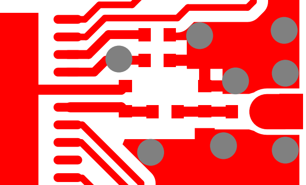
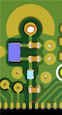
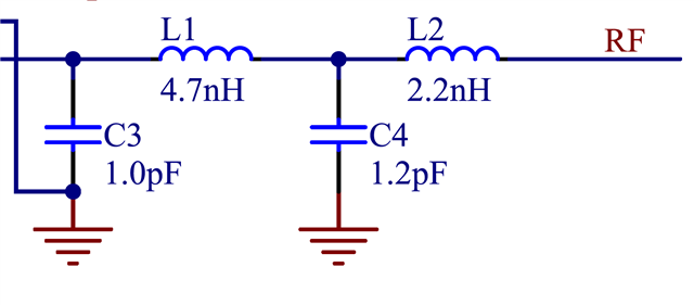
The matching network closely resembles the recommended network in the datasheet (shown in figure below). In my network, C3 = 0.8 pF, and L2 = 2.7nH due to availability of the components in our lab. 

The nRF is configured for continuous transmission on 2.4 GHz at an output power of +8 dBm.

I am measuring using a spectrum analyzer with a 50ohm input directly on the RF connector. 

The measured power is only -5 dBm, which is 13 dB lower than expected.

I understand that the cables could add some losses and that the power spec is +/-4dB, But together it shouldn't add up to 13 dB.


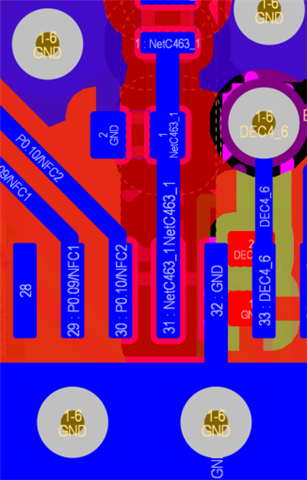
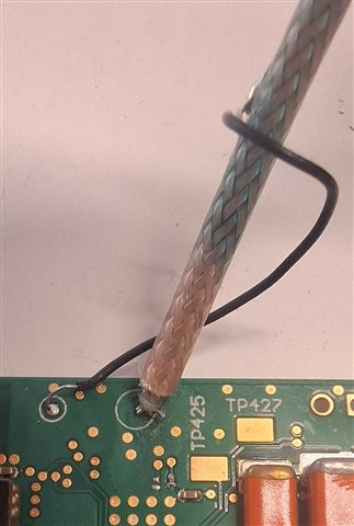
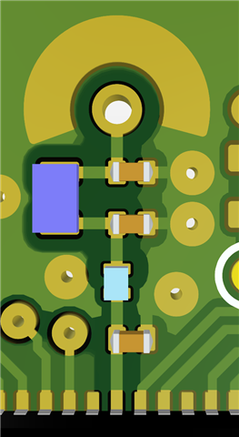
I'm also including a screenshot of the PCB. For this test, the capacitor at the output is not populated and a pigtail is soldered directly to the RF output pin to interface with the spectrum analyzer.

I would appreciate any help to identify or verify this measurement result.

Parents
  • Hi Francesc,

    The layout in the picture has several issues. The first shunt capacitor must only connect through PAVSS to the exposed pad, and must not be connected to the top GND pour. I cannot see how PAVSS is connected on your picture, could you post a screenshot in the 2D design view?

    There is also an inductor which is way too big, it should be 0201 size and placed inline with the rest of the components. Larger components have more parasitics, and could behave totally differently on high frequencies, even with the same value.

    Small deviation from the reference value could cause problems with harmonic emissions, but for the output power, there shouldn't be much difference.

    Please see the reference layout. This is how you should implement it:

    Just to be clear, at which point are you measuring the output power, in the picture below? Can you include a photo of the soldered pigtail?

    Also, what firmware are you using for the test?

Reply
  • Hi Francesc,

    The layout in the picture has several issues. The first shunt capacitor must only connect through PAVSS to the exposed pad, and must not be connected to the top GND pour. I cannot see how PAVSS is connected on your picture, could you post a screenshot in the 2D design view?

    There is also an inductor which is way too big, it should be 0201 size and placed inline with the rest of the components. Larger components have more parasitics, and could behave totally differently on high frequencies, even with the same value.

    Small deviation from the reference value could cause problems with harmonic emissions, but for the output power, there shouldn't be much difference.

    Please see the reference layout. This is how you should implement it:

    Just to be clear, at which point are you measuring the output power, in the picture below? Can you include a photo of the soldered pigtail?

    Also, what firmware are you using for the test?

Children
  • Hi Szabolcs, 

    Thank you for your reply!

    The shortest path from the first shunt capacitor to the PAVSS pin is through the ground plane on the bottom layer and coming up to the exposed pad. See the included figure.


    I am measuring at point two in your annotated screenshot. (The picture is from the backside of the pcb)


    The FW during testing is custom (developed in-house). It configures the nRF in continuous transmission mode at 2.4 GHz with the power level configured at +8 dBm.

Related