Help evaluating nrf52840 schematic

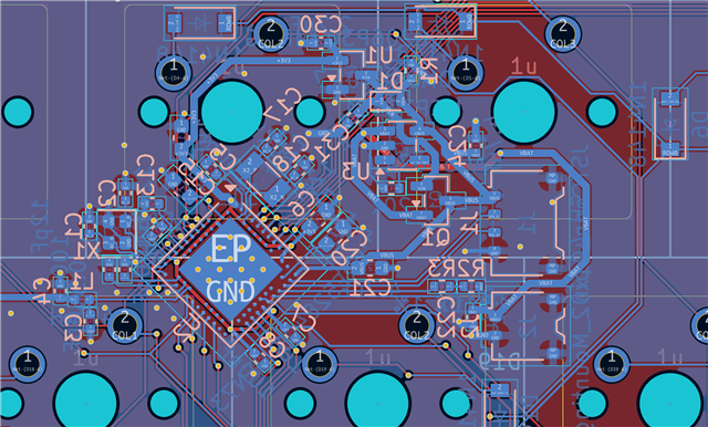
Hi, I just want to double check that I've not made any disastrous mistakes when making this keyboard. I've before used micro controller boards when designing, like nice nano, so this is my first time using the nrf52840 (aWFN73) by itself.

I've tried to follow the NRF 52840 QIAA 1_3 config 3 reference schematic as closely as I could.

I'm only doing 2 layers, other than being tricky to wire, do you think it will affect the Bluetooth or anything? I also had to short the AD12-P0.17 with the RESET button because I did not have space to trace between the pads. I guess I could do a In pad VIa, but this is fine right?

I'm using JLCPCBA BTW.

Thank you so much in advance if anyone can help me? Pray  Kissing heart

pcb_bottom.pdf1665.schema.pdf

Parents
  • 1. These components needs to be close to the ANT pin:

    Like this:

    Note how C3 here is grounded only to the VSS_PA pin and the center pad. 

    2. No tracks under the RF section, only ground plane.

    3. The VDD track on the bottom plane is creating a massive ground loop. Remove it from the ANT side of the chip.

    4. Only ground under the 32 MHz crystal. Especially the DEC4/DEC6 track must be kept away from the crystal. 

Reply
  • 1. These components needs to be close to the ANT pin:

    Like this:

    Note how C3 here is grounded only to the VSS_PA pin and the center pad. 

    2. No tracks under the RF section, only ground plane.

    3. The VDD track on the bottom plane is creating a massive ground loop. Remove it from the ANT side of the chip.

    4. Only ground under the 32 MHz crystal. Especially the DEC4/DEC6 track must be kept away from the crystal. 

Children
Related