nrf54: (Ab)using SPIM as a shift-register - between-TXLIST latency

Hi

I'm trying to drive a 75hc595-type shift register with a SPIM instance on the nrf54l15.

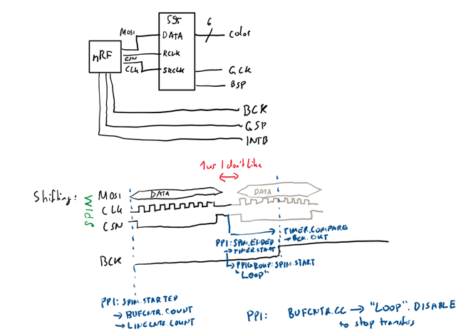
I connect MOSI to the shift register data input, CLK to the shift register clock, and CSN to the output-stage-enable register (i.e. latch from the input shifter to the output). I use the maximum frequency of the SPIM22, namely a prescaler of 2, to reach 8MHz on the output, aiming for 1 MHz output on the shift register. To set the outputs, I use EasyDMA in List mode with a MAXCNT of 1. Using CSNPOL Low, CSN is driven HIGH at the end of the transfer, thus sampling automatically into the shift register. I set IFTIMING.CSNDUR to 0.

Because I have a fixed number of bytes to sample (~240), I use a TIMER22 as a byte-counter, and a PPI group in DPPI20. I link the SPI ENDED event to the SPI STARTED event in one PPI channel, which I add to a PPIGROUP, and into the TIMER22 COUNT event. I then program a CC to the maximum number of bytes, and link it in another PPI channel to the PPIGROUP DISABLE task to break the loop and stop transferring after the programmed number of bytes.

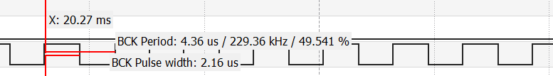
I was expecting _some_ delay caused by the CSN and rearming. But I'm observing >1us of delay between clock pulse sequences (i.e. SPI transfer active), resulting in an oscilloscope-measured time of 2us (instead of slightly more than 1us expected) between CSN pulses, halving the aimed-for frequency. Essentially, the bus idles for 1 us after every byte (which also takes 1us to transfer).

I'm a bit confused about these delays. I know that SHORTS.END_START is supposed to use IFTIMING.CSNDUR as a delay in peripheral clock cycles, so this should be 1/16 us (or 1/8 us) - not a full microsecond, so the peripheral is supposed to be faster. From what I understand from the documentation, the counter is also counting with a max delay of 1 from the PCLK, which is also 16MHz - but what I'm seeing looks like a clock of 1 MHz dominating the results.

Could you kindly point me to my mistake? I'm thinking about using the DMA TX END (rather than the SPI END) event to queue the next transfer, but I'm a bit hesitant regarding the safety of such a hack. Would the timings guarantee that the latency is enough to trigger only after the ENDED event? What would happen if the START task is triggered before (or in the same cycle where) the SPI ENDED event fires?

Is there another, better way? I was thinking about using the SPIM to transfer one array of 240 bytes at once, and pulsing the shift-latch using a different timer, but I'm a bit weary about the ultra-tight and hard-to-debug timing requirements caused by this approach given that my understanding of the PPI latencies already seems to be off.

Parents
  • Hi,


    Do you have any measurements to share, so I can see the delay? I would expect 1 us typically, based on the description in the datasheet.


    The time from .START -> actual transmission start is typically 1 us:

    https://docs.nordicsemi.com/bundle/ps_nrf54L15/page/_tmp/nrf54l15/autodita/SPIM/parameters.elec_spec.html

    And when .PSEL.CSN is configured, the timing will behave as described in the datasheet:

    https://docs.nordicsemi.com/bundle/ps_nrf54L15/page/spim.html#ariaid-title4


    Ie. you will get a delay before- and after a transmission, thus you will see a "double delay" between each transaction (one byte in your scenario).

    I set IFTIMING.CSNDUR to 0.

    If we look at the definition of this register:

    https://docs.nordicsemi.com/bundle/ps_nrf54L15/page/spim.html#ariaid-title59

    it mentions specifically:

    Note that for low values of CSNDUR, the system turnaround time will dominate the actual time between transactions


    Kind regards,

    Håkon

  • Hi

    I apologize for the delay.
    Unfortunately, I currently only have access to the capture of a pin (BCK) toggled at a fixed delay after the SPI end. This is expected to read ~1us for every transaction when considering the raw transmission time.

    Your mention of the 1us START delay explains the other 1us of delay between the transfers.

    I find the datasheet a bit confusing regarding the CSNDUR, especially because the timing diagram in Figure 4 does not actually include this "turnaround" time. Is the time of "CSN high" a function of min(1us, CSNDUR*(1/PCLK))? Or 1us + CSNDUR*(1/PLK)? And does this 1us START delay apply also with SHORTS.ENDED_START ?

    Considering my usecase, would it be possible to PPI a pin to pulse the "CSN" pin (then disconnected from the SPI) precisely after the last bit has been asserted and the CLK has sampled? Specifically, is the SHORT on the TIMER clear constant in time, and is the peripheral clock of one domain synched?
    Or is there a "best practice" to implement the SRCLK signal on a 595-type IC in sync with the SPI peripheral?

    Kind regards

  • Hi,


    I would strongly recommend that you look at the different signals to see how they behave, it'll be a lot easier for you if you are able to see how and where the delays propagate through the system

    cwriter said:
    Unfortunately, I currently only have access to the capture of a pin (BCK) toggled at a fixed delay after the SPI end. This is expected to read ~1us for every transaction when considering the raw transmission time.

    Transmission takes 1 us, and from TASKS_START =1 to actual transmission is typically 1 us. This seems to add up, as you measure 2.16 us, unless I am reading this incorrectly?

    cwriter said:
    I find the datasheet a bit confusing regarding the CSNDUR, especially because the timing diagram in Figure 4 does not actually include this "turnaround" time. Is the time of "CSN high" a function of min(1us, CSNDUR*(1/PCLK))? Or 1us + CSNDUR*(1/PLK)? And does this 1us START delay apply also with SHORTS.ENDED_START ?

    Figure 4 shows that there is a delay when asserting and when de-asserting the CSN pin, as per the configured CSNDUR duration.

    cwriter said:
    Considering my usecase, would it be possible to PPI a pin to pulse the "CSN" pin (then disconnected from the SPI) precisely after the last bit has been asserted and the CLK has sampled? Specifically, is the SHORT on the TIMER clear constant in time, and is the peripheral clock of one domain synched?

    I think it would be easier if you share a picture of what you're ideally want to implement, and share that.

    I might be misunderstanding what you're doing here, but:

    When reading the application, my immediate question is; How should the CSN be toggled if you expect to send continuously?


    So, you can use PPI to toggle a pin based on start/stop, but you will also need to add a timer instance or similar to let the csn pin return to idle for a small period of time.


    Kind regards,

    Håkon

  • Hi

    I think it would be easier if you share a picture of what you're ideally want to implement, and share that.

    I apologize if I was being unclear. I tried to abstract the problem to the smallest possible component, which I realize may have been confusing.

    I'm trying to drive a somewhat complex Display:

    https://www.sharpsecd.com/static/media/LS021B7DD02_Spec_LCP-0620032_201201.5be4ecdb4b72073f1e52.pdf

    To conserve precious pin state, the hardware design uses a 595 shift IC to assert the datalines.
    The sharp datasheet lists very strict timings, but at least a few tested samples seem to be quite lenient and can tolerate a slower clock (at the cost of lower frame rates, which is acceptable).

    I've added a rough overview on how I'm driving the system. A goal is to not have the CPU involved in the transfers, hence I'm using the PPI interface.

    In summary, I'm using the SPIM in DMA.TXLIST mode to emit 1 byte, then assert CSN (which moves from the 595's input register to the output), then start the next transfer using a PPI group.
    At the end of each byte, the SPIM auto-sets CSN, which asserts the input register of the 595 to the outputs. I then use a timer to delay the BCK toggle (which samples the outputs into the display) to roughly the middle of the following transfer. Because of the TXLIST, the DMA pointer is advanced, and the next transfer will transfer the next byte.
    The PPI group is disabled when the counter reaches the specified amount of bytes, therefore disconnecting the loop. 
    Essentially, this allows me to transfer a "frame buffer" (which also contains the control signals) from RAM without any CPU intervention. During the special frame start / frame end sequences of the display, I'm currently using an IRQ state machine for now.
    The linking of PPI to actual "byte end" events allows for precise timing of the signals. If I was to transfer thousands of bytes, I'm worried that hard-coding timer values might skew when the DMA delays ever so slightly, and the skew leading to imprecise signals towards the end of the transfer.

    The result is qualitatively correct, but the timings are stretched due to the delay between the SPI transfers. Hence, the question is how I can reduce this delay.

    The stretched clocks on GCK / delays between the blocks of BCK are due to an interrupt which gradually releases chunks of the ring buffer; I'll optimize this later.

    The sharp data sheet is a bit weird in that it does not list a minimum frequency but lists tight pulse width levels that correspond exactly to the frequency. I'm fine driving this out of spec: Using this setup, the maximum frequency I can achieve on BCK is 0.5 MHz (instead of 0.746 MHz) - this is fine. However, due to the added delay between the SPI transfers, the frequency of BCK is a measured ~230 kHz, and I'd like to improve this value.

    I would strongly recommend that you look at the different signals to see how they behave, it'll be a lot easier for you if you are able to see how and where the delays propagate through the system

    Sorry if I was unclear. I looked at them and I know how they behave. I'm trying to figure out how I can make them behave differently.

    Transmission takes 1 us, and from TASKS_START =1 to actual transmission is typically 1 us. This seems to add up, as you measure 2.16 us, unless I am reading this incorrectly?

    This is also my understanding. The question I have is how it's possible to remove this 1us delay after TASKS_START (or hide it by starting the work earlier)

    Figure 4 shows that there is a delay when asserting and when de-asserting the CSN pin, as per the configured CSNDUR duration.

    Exactly. But it does not show a 1us delay (it does not say "CSNDUR + turnaround time"), which is why I was wondering if this 1us delay can be skipped somehow (and what the CSN high period was if CSNDUR=0). Hence; the question is if this delay does not apply when using SHORTS - and if it does, how I can precisely stop the ever-looping SHORTS mode after n transmissions.

    When reading the application, my immediate question is; How should the CSN be toggled if you expect to send continuously?

    CSN is toggled after each transfer. I use TXLIST mode with MAXCNT=1 to have ~240 bytes * (number of buffered lines) transferred, the CSN pin rises after each byte (which is the sampling signal for the RCLK pin on the 595). Ideally, there would be just 1 SPI clock cycle (~1/8us) of CSN high, before the next transfer is triggered - or, in absolute times, the hold time of the 595 is 24ns - so CSN high can last essentially arbitrarily short, but it must be (stably) high before the next transfer. 

    So, you can use PPI to toggle a pin based on start/stop, but you will also need to add a timer instance or similar to let the csn pin return to idle for a small period of time.

    Yes, but I'm not sure how I could ensure this setup works in case of DMA stalls, and when using START/STOP, I'd still run into the issue of the 1us delay between data transfers - this infamous 1us - or did I misunderstand this?

    Kind regards

Reply
  • Hi

    I think it would be easier if you share a picture of what you're ideally want to implement, and share that.

    I apologize if I was being unclear. I tried to abstract the problem to the smallest possible component, which I realize may have been confusing.

    I'm trying to drive a somewhat complex Display:

    https://www.sharpsecd.com/static/media/LS021B7DD02_Spec_LCP-0620032_201201.5be4ecdb4b72073f1e52.pdf

    To conserve precious pin state, the hardware design uses a 595 shift IC to assert the datalines.
    The sharp datasheet lists very strict timings, but at least a few tested samples seem to be quite lenient and can tolerate a slower clock (at the cost of lower frame rates, which is acceptable).

    I've added a rough overview on how I'm driving the system. A goal is to not have the CPU involved in the transfers, hence I'm using the PPI interface.

    In summary, I'm using the SPIM in DMA.TXLIST mode to emit 1 byte, then assert CSN (which moves from the 595's input register to the output), then start the next transfer using a PPI group.
    At the end of each byte, the SPIM auto-sets CSN, which asserts the input register of the 595 to the outputs. I then use a timer to delay the BCK toggle (which samples the outputs into the display) to roughly the middle of the following transfer. Because of the TXLIST, the DMA pointer is advanced, and the next transfer will transfer the next byte.
    The PPI group is disabled when the counter reaches the specified amount of bytes, therefore disconnecting the loop. 
    Essentially, this allows me to transfer a "frame buffer" (which also contains the control signals) from RAM without any CPU intervention. During the special frame start / frame end sequences of the display, I'm currently using an IRQ state machine for now.
    The linking of PPI to actual "byte end" events allows for precise timing of the signals. If I was to transfer thousands of bytes, I'm worried that hard-coding timer values might skew when the DMA delays ever so slightly, and the skew leading to imprecise signals towards the end of the transfer.

    The result is qualitatively correct, but the timings are stretched due to the delay between the SPI transfers. Hence, the question is how I can reduce this delay.

    The stretched clocks on GCK / delays between the blocks of BCK are due to an interrupt which gradually releases chunks of the ring buffer; I'll optimize this later.

    The sharp data sheet is a bit weird in that it does not list a minimum frequency but lists tight pulse width levels that correspond exactly to the frequency. I'm fine driving this out of spec: Using this setup, the maximum frequency I can achieve on BCK is 0.5 MHz (instead of 0.746 MHz) - this is fine. However, due to the added delay between the SPI transfers, the frequency of BCK is a measured ~230 kHz, and I'd like to improve this value.

    I would strongly recommend that you look at the different signals to see how they behave, it'll be a lot easier for you if you are able to see how and where the delays propagate through the system

    Sorry if I was unclear. I looked at them and I know how they behave. I'm trying to figure out how I can make them behave differently.

    Transmission takes 1 us, and from TASKS_START =1 to actual transmission is typically 1 us. This seems to add up, as you measure 2.16 us, unless I am reading this incorrectly?

    This is also my understanding. The question I have is how it's possible to remove this 1us delay after TASKS_START (or hide it by starting the work earlier)

    Figure 4 shows that there is a delay when asserting and when de-asserting the CSN pin, as per the configured CSNDUR duration.

    Exactly. But it does not show a 1us delay (it does not say "CSNDUR + turnaround time"), which is why I was wondering if this 1us delay can be skipped somehow (and what the CSN high period was if CSNDUR=0). Hence; the question is if this delay does not apply when using SHORTS - and if it does, how I can precisely stop the ever-looping SHORTS mode after n transmissions.

    When reading the application, my immediate question is; How should the CSN be toggled if you expect to send continuously?

    CSN is toggled after each transfer. I use TXLIST mode with MAXCNT=1 to have ~240 bytes * (number of buffered lines) transferred, the CSN pin rises after each byte (which is the sampling signal for the RCLK pin on the 595). Ideally, there would be just 1 SPI clock cycle (~1/8us) of CSN high, before the next transfer is triggered - or, in absolute times, the hold time of the 595 is 24ns - so CSN high can last essentially arbitrarily short, but it must be (stably) high before the next transfer. 

    So, you can use PPI to toggle a pin based on start/stop, but you will also need to add a timer instance or similar to let the csn pin return to idle for a small period of time.

    Yes, but I'm not sure how I could ensure this setup works in case of DMA stalls, and when using START/STOP, I'd still run into the issue of the 1us delay between data transfers - this infamous 1us - or did I misunderstand this?

    Kind regards

Children
No Data
Related