I am designing an ultra-low-power BLE Audio TWS board based on the nRF5340 and have followed the recommended hardware design guidelines throughout the project. This is my final design, and I would appreciate a review.
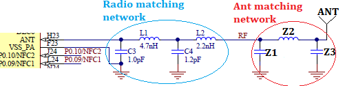
- For the Bluetooth antenna matching network, are any additional components required, or is the current configuration sufficient? The antenna will be implemented directly on the PCB. Specificaly do i need the extended antenna matching part?
- This is currently a test board, but the final version will need to be significantly smaller. At the moment, there are quite a few decoupling capacitors included in the design. Which ones are essential, and which could potentially be removed or reduced to save space?
The scematic PDF:
8081.MSBE_V3.pdf