Hi,
1.The customer does not require an external hardware reset circuit. How should the reset pin be handled externally?
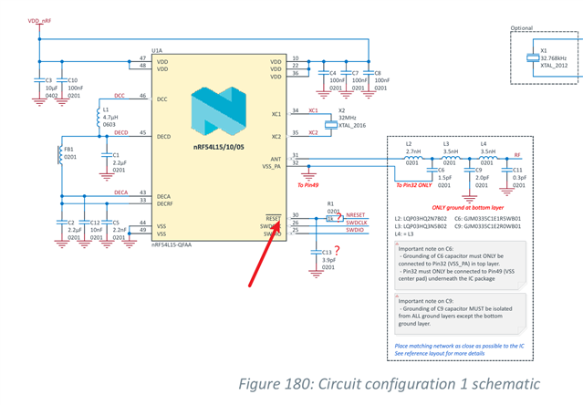
2. Can R1 and C13 be omitted?
3. If R1 cannot be omitted? So, should R1 be left dangling?
Best regards,
Peter.Min
Hi,
1.The customer does not require an external hardware reset circuit. How should the reset pin be handled externally?
2. Can R1 and C13 be omitted?
3. If R1 cannot be omitted? So, should R1 be left dangling?
Best regards,
Peter.Min