Can the same BLE antenna and matching network be reused across nRF52, nRF53, and nRF54 Series devices?

Hello Nordic Team,

I am designing a custom PCB using the nRF52840 and a PCB trace antenna for 2.4 GHz BLE.

In my current design:

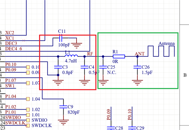
I will take nRF52840 dongle antenna design, impedance matching circuit and LC filter without any changes.

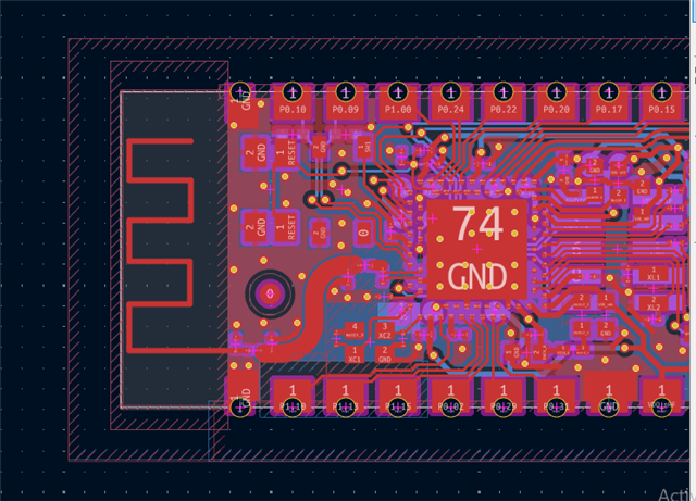
I have attached a screenshot of my RF layout showing:

  • nRF52840 RF pin
  • Matching network components
  • RF trace routing
  • PCB antenna feed trace

My question is about reusing the antenna design on other Nordic devices.

If I replace the nRF52840 with another Nordic SoC such as:

  • nRF52832
  • nRF5340
  • nRF54L05
  • nRF54L10
  • nRF54L15

Can I reuse the same PCB antenna geometry and antenna feed layout, or is a new antenna design and matching network required for each device?

I understand that all devices operate in the 2.4 GHz band, but I would like to know:

  1. Whether the antenna geometry can remain unchanged.
  2. Whether the RF matching components must be redesigned for each SoC.
  3. Whether Nordic provides guidance on reusing antenna designs across different SoC families.

Thank you.

Parents
  • Hi,

    The antenna can be of course reused. It it a generic PILA design for the 2.4GHz bands. All of the chips you listed use this frequency band, so the antenna is good for these. (For our other products, like the nRF9151, you would need completely different antennas.)

    Regarding the matching network, there are actually two of this, as you see in the schematic below. One is specific to this antenna (green) and the other is specific for the chip (red).

    The matching for the chip is specific to the IC. The schematic, the component values and sizes, and the layout must follow the reference for the corresponding chip. These components are placed close to the chip.

    The antenna matching is however there to tune the antenna. Here, there is a mounting option for a pi network, but only a shunt capacitor is used, which is usually enough to tune this kind of antenna design. These components must be placed close to the antenna. The antenna's and the chip's matching network is connected by a 50 Ohm impedance controlled transmission line (labeled "RF" here).

    Please note, that if your custom PCB size is different than the dongle, then the antenna tuning might need to be adjusted. This is usually done by changing the capacitor value (C26), and/or by adjusting the trace length of the antenna. Nordic offers this tuning as a free service for our customers.

    I strongly recommend opening a hardware review case here once your PCB design is finalized, so we Nordic engineers can confirm that your design does not have any RF issues.

    To summarize your questions:

    1. Yes, it can.
    2. The matching for the chip must be always corresponding to the Reference Layout. The antenna matching (usually just one capacitor) depends on the PCB geometry.
    3. Most of our antenna designs can be used for custom boards, but they might need retuning.
  • Hello,

    Thank you very much for your detailed reply. It helped me understand the difference between the SoC matching network and the antenna matching network.

    I have a few additional questions:

    1. If I keep the same antenna design and the same MCU section, but reduce the overall PCB size, will the antenna still require retuning?

    For example, if the antenna geometry, matching components, and RF trace remain unchanged, but the PCB dimensions become smaller than the original nRF52840 Dongle board, how much impact can this have on antenna performance?

    Since I do not have RF test equipment such as a VNA or spectrum analyzer, how can I determine whether tuning is required? Is there any recommended design approach to minimize the need for retuning while maintaining 2.4 GHz operation and a 50 Ω transmission line?

    1. Regarding the nRF52840 Dongle reference design:

    Is the nRF52840 Dongle a certified design?

    If yes:

    • Which certifications does it have (FCC, CE, IC, etc.)?
    • Are the certification reports publicly available?

    I would like to better understand whether using the nRF52840 Dongle antenna and RF layout as a reference can help simplify the certification process for a custom PCB design.

    Thank you again for your support.

Reply
  • Hello,

    Thank you very much for your detailed reply. It helped me understand the difference between the SoC matching network and the antenna matching network.

    I have a few additional questions:

    1. If I keep the same antenna design and the same MCU section, but reduce the overall PCB size, will the antenna still require retuning?

    For example, if the antenna geometry, matching components, and RF trace remain unchanged, but the PCB dimensions become smaller than the original nRF52840 Dongle board, how much impact can this have on antenna performance?

    Since I do not have RF test equipment such as a VNA or spectrum analyzer, how can I determine whether tuning is required? Is there any recommended design approach to minimize the need for retuning while maintaining 2.4 GHz operation and a 50 Ω transmission line?

    1. Regarding the nRF52840 Dongle reference design:

    Is the nRF52840 Dongle a certified design?

    If yes:

    • Which certifications does it have (FCC, CE, IC, etc.)?
    • Are the certification reports publicly available?

    I would like to better understand whether using the nRF52840 Dongle antenna and RF layout as a reference can help simplify the certification process for a custom PCB design.

    Thank you again for your support.

Children
No Data
Related