![]()
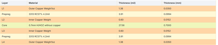
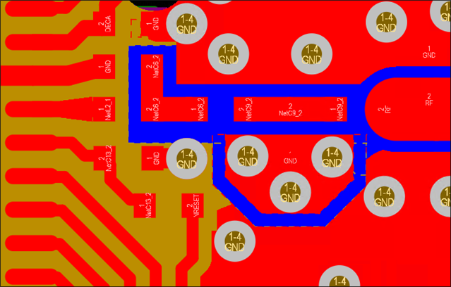
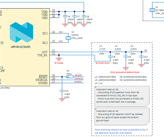
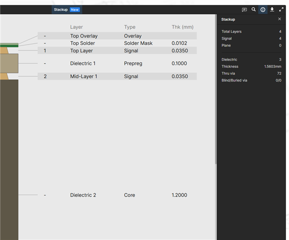
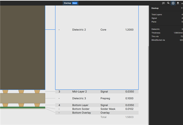
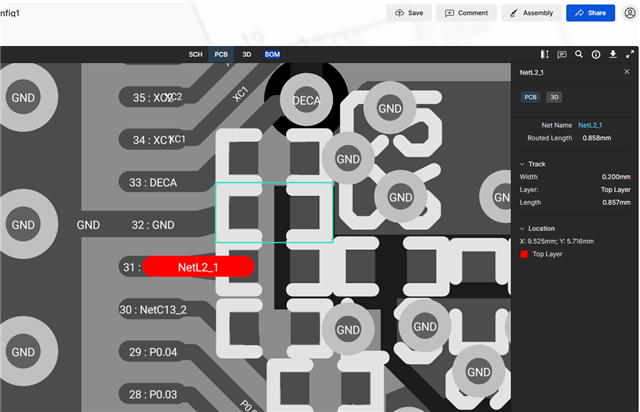
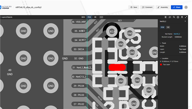
So I have two questions. My first is on the impedance matching network on different pcb stackups. So wouldn't I need a different matching network for a different pcb stackup? The reference design uses a 1.6mm board with 4.6 dielectric constant. While I'm using a 1mm board with 4.5 dielectric constant. Is there way I can do simulations before manufacturing the pcb? Second question is why are the widths different for the traces in the impedance matching network? Like it goes from 0.2mm to 0.27mm to 0.3mm. Why 0.3mm. I get why transmission trace is 0.762 because that is 50 ohms for the pcb stackup.