nPM1300 BUCK2 not regulating to 3.3 V in standalone mode

Hi Nordic team,

I'm debugging a custom board using the nPM1300 and I'm seeing unexpected behavior from BUCK2. I'd appreciate any guidance on whether I'm misunderstanding the VSET configuration or if there is another startup/configuration requirement that I'm missing.

Hardware Configuration

  • PMIC: nPM1300

  • Operating mode: Standalone (no PMIC configuration over I²C)

  • BUCK2 desired output: 3.3 V

  • VSET2 resistor: 300 kΩ to GND

  • According to the nPM1300 Product Specification v1.3, the VSET2 table shows:

    • 250–500 kΩ → 3.3 V

  • NTC pin connected to GND through a 0 Ω resistor

  • No intentional connection between BUCK2 output and VSYS

  • Resistance from VSET2 to GND measures approximately 300 kΩ on the board

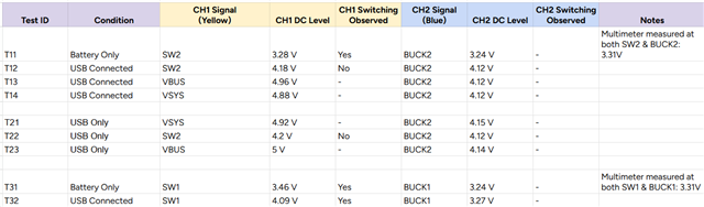
Observed Behavior (Board Under Test)

With USB power connected:

Signal Measured Voltage
VBUS 5.1 V
VSYS 5.0 V
BUCK2 Output (VOUT2) 4.45 V

The expected BUCK2 output is 3.3 V, but instead it sits around 4.45 V.

Battery-only operation

When running from battery:

  • One board measures ~3.3 V at BUCK2 output

  • Another board measures ~3.5 V at BUCK2 output

The output appears to track the battery voltage rather than regulate to a fixed 3.3 V.

Questions

  1. Is 300 kΩ a valid VSET2 value for selecting 3.3 V on nPM1300 Product Specification v1.3?

  2. In standalone mode, should BUCK2 automatically enable and regulate to the VSET-selected voltage at startup?

  3. Could grounding the NTC pin through 0 Ω affect BUCK2 startup or operation?

  4. Is it expected that VSYS measures almost the same as VBUS (5.0 V vs 5.1 V) in this configuration?

  5. Are there any recommended measurements or status registers that would help determine whether BUCK2 is actually enabled?

Any suggestions for further debugging would be greatly appreciated.

Thank you.

Parents
  • Hi,

    This sound like an issue, the nPM should start the Buck automatically with the configuration you stated. Can you please post your schematic?

    Regarding your questions:

    1. Yes,
    2. Yes.
    3. I think it shouldn't, but you can try replacing it with a 10K resistor just for debugging purposes. If there is no NTC for the battery, this feature should be disabled in the register, but I think it only affects battery charging, and not the Bucks.
    4. Yes, there is no regulator behind VSYS, it is only a current-limited output.
    5. Yes, see BUCKSTATUS and BUCK2VOUTSTATUS.
  • Dear Szabolcs,

    Thank you for your response and for clarifying the questions.

    Please find the complete schematic attached to this ticket for your review.

    https://devzone.nordicsemi.com/support/359762

    Kindly review the schematic and let me know if you notice anything that could prevent BUCK2 from starting or regulating correctly?

    Thank you for your support.

    Regards,

    Tarun

  • Additional information from testing:


    I am able to communicate with the nPM1300 successfully over I²C.

    Using the regulator shell commands, I can query the PMIC and obtain the following:

    regulator vget BUCK1
    3.300000 V
    
    regulator vget BUCK2
    3.300000 V

    So there appears to be a discrepancy between the PMIC-reported BUCK2 voltage setting (3.3 V) and the physical voltage measured on the BUCK2 output (3.33 V) when LiPo Battery only connected state.

    Then I connected USB to give the VBUS supply when battery connected, immediately the voltage on VBUCK2 changed to 4.2V. Still I could see the I2C communication active.

    Current consumption shows: 90-110mA in the USB power-meter

    Please let me know any insights.

    Thank you

  • Queries:

    • Any OTP/factory-programmed settings exist.
    • Any retained configuration can override VSET startup behavior.
  • Hi,

    thank you for the extra information. I see that you have the designed reviewed, I double checked it just in case, but it is OK, I don't see any obvious issues that could cause this.

    The nPM reporting 3.3V makes sense, as this is the maximum voltage for the Bucks, so anything higher is probably over the measurement limit.

    There is no OTP or retained registers in the nPM, I think it does not have any memory at all, so a reset should always bring it to the same state.

    The current consumption is suspiciously high. The default current limit is 100 mA, so the nPM is probably in current limiting mode. Could you double check your board for short circuits, soldering issues, etc.? (I see in your other ticket that you needed rework.)

    Do all of your board have the rework? Do all of them produce the same symptoms?

    Can you make oscilloscope measurements? Seeing VBUS, VSYS, and the buck output and SW lines on startup would be helpful.

  • Dear Szabolcs,

    Thank you for reviewing the schematic and for your feedback.

    Regarding the current consumption, I would like to clarify that the measured current on the boards under test is approximately 30 - 33 mA with VBUS connected, which appears to be well below the default 100 mA current limit. Please disregard the earlier estimate of 90–110 mA that I mentioned during the initial investigation with some external debug tools connected, as subsequent measurements indicate the current consumption is significantly lower.

    Regarding the rework, yes, the boards currently being tested have undergone rework to remove the compass device. However, the BUCK2 behavior remains consistent across the tested boards (6 Boards):

    • Battery only: BUCK2 / 3V3A ≈ 3.294 - 3.33 V
    • VBUS connected: BUCK2 / 3V3A ≈ 4.24 V

    I will share the scope measurements/waveforms of VBUS, VSYS, BUCK2 output, and SW2 during startup soon.

    Regards,

  • Dear Szabolcs,

    Could you review the complete register dump attached, along with some manual measurements and observations included at the end of the document. Please let me know if you notice anything unexpected or any configuration that warrants further investigation.

    ## Register dump
    
    NPM13XX_REGISTER_DUMP_BEGIN
    MAIN page 0x00 (0x00..0x27)
      0000: 00 00 ff ff 00 00 2c 2c 00 00 06 06 00 00 00 00
      0010: 00 00 00 00 03 03 3d 3d 00 00 00 00 00 00 00 00
      0020: 00 00 00 00 00 00 02 02
    VBUS/LDSW_EXTRA page 0x02 (0x00..0x0c)
      0200: 00 01 05 00 00 00 00 21 00 00 00 00 00
    CHARGER page 0x03 (0x00..0x50)
      0300: 00 00 00 00 01 01 02 02 08 00 cf 01 07 04 00 00
      0310: bb 01 a4 02 54 01 3b 01 5a 00 5d 00 00 00 00 00
      0320: 00 00 00 00 00 00 00 00 00 00 00 00 44 00 00 00
      0330: 00 10 00 00 09 0e 00 00 0d 0c 08 07 00 00 0e 04
      0340: 03 02 00 03 00 01 26 00 00 00 00 00 0c 07 00 00
      0350: 00
    BUCK page 0x04 (0x00..0x35)
      0400: 00 00 00 00 00 00 00 00 17 02 08 08 41 00 00 01
      0410: 17 17 03 03 00 00 00 00 00 00 00 00 00 00 c2 00
      0420: c2 00 00 00 00 00 1d 1d 03 1e 00 5f 01 06 1f 1e
      0430: 5d 02 00 00 44 00
    ADC page 0x05 (0x00..0x24)
      0500: 00 00 00 00 00 00 00 00 00 00 00 03 00 00 00 01
      0510: 0f ca 00 6d c1 01 00 de 00 a6 90 00 00 00 00 00
      0520: 1a 17 1a 3c 01
    GPIO page 0x06 (0x00..0x1e)
      0600: 00 09 00 05 00 00 00 00 00 00 00 00 00 00 00 01
      0610: 00 01 01 01 00 00 00 00 00 00 00 00 00 00 00
    TIMER page 0x07 (0x00..0x0a)
      0700: 00 00 00 00 00 00 02 00 00 00 00
    LDSW page 0x08 (0x00..0x0d)
      0800: 00 00 00 00 12 0a 0a 00 01 01 00 01 17 08
    POF page 0x09 (0x00..0x00)
      0900: 00
    LEDDRV page 0x0a (0x00..0x08)
      0a00: 02 02 02 00 00 00 00 00 00
    SHIP page 0x0b (0x00..0x07)
      0b00: 00 00 00 00 03 01 01 00
    ERRLOG page 0x0e (0x00..0x05)
      0e00: 00 00 00 00 00 00
    NPM13XX_REGISTER_DUMP_END
    
    ## Parsing Register Dump
    
    NPM13XX_ANALYSIS_BEGIN
    PMIC: part=nPM1300 revision=0x02.2 rstcause=0x00 ship_exit=no boot_monitor=no watchdog=no longpress=no unknown=0x00
    VBUS: present status=0x21 detect=0x00 (no source detected) current_limit=no ovp=no uv=no suspended=no busout=yes
    VBUS config: ilim0=0x01 (100 mA) startup=0x05 (500 mA) suspend=0x00
    Charger: status=0x09 (constant-current) iset=0x08.0 (32.000 mA) vterm_idx=0x07 (4150 mV) vterm_r_idx=0x04 (4000 mV)
    Charger aux: ilim_status=0x00 ntc_status=0x00 die_status=0x00 disable=0x02 recharge_disabled=no ntc_disabled=yes config=0x00 vbatlow_charge=0x00 (disabled)
    Charger error reason: none
    Charger error sensor: none
    ERRLOG charger: reason=0x00 sensor=0x00
    BUCK2: on=yes status=0x44 sw_control=no selected_idx=0x17 (3300 mV) vout_norm=0x08 (1800 mV) vout_stat=0x17 (3300 mV) retention=0x08 (1800 mV)
    BUCK control: ctrl0=0x00 en_ctrl=0x41 vret_ctrl=0x00 pwm_ctrl=0x00 sw_ctrl=0x01
    BUCK2 range note: nPM13xx BUCK/LDO selectors cover 1000..3300 mV; no register setting can command 4100 mV.
    POF: config=0x00 state=disabled polarity_high=no threshold_idx=0x00 (2800 mV)
    GPIO: status=0x00 gpio0=no gpio1=no gpio2=no gpio3=no gpio4=no
    LEDDRV: mode0=0x02 (host) mode1=0x02 (host) mode2=0x02 (host)
    LDSW: status=0x12 ldo1_on=yes ldo2_on=no config=0x00 ldo1_mode=LDO ldo2_mode=LDO ldo1_vout_idx=0x17 (3300 mV) ldo2_vout_idx=0x08 (1800 mV)
    ADC: vbat_raw=809 -> 3950 mV vsys_raw=770 -> 4793 mV vbus_raw=664 -> 4863 mV ntc_raw=0 die_raw=437 ibat_raw=1 ibat_stat=0x0f config=0x00 auto=0x00 (disabled) ibat_en=0x01 (enabled)
    NPM13XX_ANALYSIS_END
    
    ## Manual Observations
    
    ### VBUS ON + VBAT ON
    BUCK2 = 4.1v - NOT_AS_PER_EXPECTATION
    BUCK1 disable / enable via shell is reflecting on pcb correctly. NOTE: voltage is very slowly reducing when disabled.
    LDO2 disable / enable via shell is reflecting on pcb correctly. NOTE: voltage is very slowly reducing when disabled.
    LDO1 disabled = 2.8v and enable = 3.285v - NOT_AS_PER_EXPECTATION
    
    ### VBUS ON + VBAT OFF
    BUCK2 = 4.1v - NOT_AS_PER_EXPECTATION
    BUCK1 disable / enable via shell is reflecting on pcb correctly. NOTE: voltage is very slowly reducing when disabled.
    LDO2 disable / enable via shell is reflecting on pcb correctly. NOTE: voltage is very slowly reducing when disabled.
    LDO1 disabled = 2.8v and enable = 3.285v - NOT_AS_PER_EXPECTATION
    
    ### VBUS OFF + VBAT ON
    BUCK2 = 3.3v
    BUCK1 disable / enable via shell is reflecting on pcb correctly. NOTE: voltage is very slowly reducing when disabled.
    LDO2 disable / enable via shell is reflecting on pcb correctly. NOTE: voltage is very slowly reducing when disabled.
    LDO1 disabled = 2.8v and enable = 3.285v - NOT_AS_PER_EXPECTATION


    While continuing the investigation, we wanted to cross-check a few points from the datasheet to ensure we are not overlooking any configuration-related causes:

    1. In our design, VBUSOUT is connected directly to the nRF5340 VBUS pin as recommended. Is there any possibility that the VBUSOUT path or VBUS detection circuitry could influence BUCK2 behavior when USB is connected?
    2. We are not intentionally using USB Selective Suspend (VBUSSUSPEND). The datasheet states that VBUS can be disconnected from VSYS while VBUSOUT remains active in this mode. Could this functionality affect BUCK operation in any way, or can it be ruled out for the observed behavior?
    3. Can charge-related settings such as ICHG (charge current limit) or VTERMSET (termination voltage) be ruled out as possible contributors to the observed BUCK2 behavior, or are there any known interactions between the charger and BUCK regulators that should be considered during debugging?

    Thank you for your guidance.

    Regards,

Reply
  • Dear Szabolcs,

    Could you review the complete register dump attached, along with some manual measurements and observations included at the end of the document. Please let me know if you notice anything unexpected or any configuration that warrants further investigation.

    ## Register dump
    
    NPM13XX_REGISTER_DUMP_BEGIN
    MAIN page 0x00 (0x00..0x27)
      0000: 00 00 ff ff 00 00 2c 2c 00 00 06 06 00 00 00 00
      0010: 00 00 00 00 03 03 3d 3d 00 00 00 00 00 00 00 00
      0020: 00 00 00 00 00 00 02 02
    VBUS/LDSW_EXTRA page 0x02 (0x00..0x0c)
      0200: 00 01 05 00 00 00 00 21 00 00 00 00 00
    CHARGER page 0x03 (0x00..0x50)
      0300: 00 00 00 00 01 01 02 02 08 00 cf 01 07 04 00 00
      0310: bb 01 a4 02 54 01 3b 01 5a 00 5d 00 00 00 00 00
      0320: 00 00 00 00 00 00 00 00 00 00 00 00 44 00 00 00
      0330: 00 10 00 00 09 0e 00 00 0d 0c 08 07 00 00 0e 04
      0340: 03 02 00 03 00 01 26 00 00 00 00 00 0c 07 00 00
      0350: 00
    BUCK page 0x04 (0x00..0x35)
      0400: 00 00 00 00 00 00 00 00 17 02 08 08 41 00 00 01
      0410: 17 17 03 03 00 00 00 00 00 00 00 00 00 00 c2 00
      0420: c2 00 00 00 00 00 1d 1d 03 1e 00 5f 01 06 1f 1e
      0430: 5d 02 00 00 44 00
    ADC page 0x05 (0x00..0x24)
      0500: 00 00 00 00 00 00 00 00 00 00 00 03 00 00 00 01
      0510: 0f ca 00 6d c1 01 00 de 00 a6 90 00 00 00 00 00
      0520: 1a 17 1a 3c 01
    GPIO page 0x06 (0x00..0x1e)
      0600: 00 09 00 05 00 00 00 00 00 00 00 00 00 00 00 01
      0610: 00 01 01 01 00 00 00 00 00 00 00 00 00 00 00
    TIMER page 0x07 (0x00..0x0a)
      0700: 00 00 00 00 00 00 02 00 00 00 00
    LDSW page 0x08 (0x00..0x0d)
      0800: 00 00 00 00 12 0a 0a 00 01 01 00 01 17 08
    POF page 0x09 (0x00..0x00)
      0900: 00
    LEDDRV page 0x0a (0x00..0x08)
      0a00: 02 02 02 00 00 00 00 00 00
    SHIP page 0x0b (0x00..0x07)
      0b00: 00 00 00 00 03 01 01 00
    ERRLOG page 0x0e (0x00..0x05)
      0e00: 00 00 00 00 00 00
    NPM13XX_REGISTER_DUMP_END
    
    ## Parsing Register Dump
    
    NPM13XX_ANALYSIS_BEGIN
    PMIC: part=nPM1300 revision=0x02.2 rstcause=0x00 ship_exit=no boot_monitor=no watchdog=no longpress=no unknown=0x00
    VBUS: present status=0x21 detect=0x00 (no source detected) current_limit=no ovp=no uv=no suspended=no busout=yes
    VBUS config: ilim0=0x01 (100 mA) startup=0x05 (500 mA) suspend=0x00
    Charger: status=0x09 (constant-current) iset=0x08.0 (32.000 mA) vterm_idx=0x07 (4150 mV) vterm_r_idx=0x04 (4000 mV)
    Charger aux: ilim_status=0x00 ntc_status=0x00 die_status=0x00 disable=0x02 recharge_disabled=no ntc_disabled=yes config=0x00 vbatlow_charge=0x00 (disabled)
    Charger error reason: none
    Charger error sensor: none
    ERRLOG charger: reason=0x00 sensor=0x00
    BUCK2: on=yes status=0x44 sw_control=no selected_idx=0x17 (3300 mV) vout_norm=0x08 (1800 mV) vout_stat=0x17 (3300 mV) retention=0x08 (1800 mV)
    BUCK control: ctrl0=0x00 en_ctrl=0x41 vret_ctrl=0x00 pwm_ctrl=0x00 sw_ctrl=0x01
    BUCK2 range note: nPM13xx BUCK/LDO selectors cover 1000..3300 mV; no register setting can command 4100 mV.
    POF: config=0x00 state=disabled polarity_high=no threshold_idx=0x00 (2800 mV)
    GPIO: status=0x00 gpio0=no gpio1=no gpio2=no gpio3=no gpio4=no
    LEDDRV: mode0=0x02 (host) mode1=0x02 (host) mode2=0x02 (host)
    LDSW: status=0x12 ldo1_on=yes ldo2_on=no config=0x00 ldo1_mode=LDO ldo2_mode=LDO ldo1_vout_idx=0x17 (3300 mV) ldo2_vout_idx=0x08 (1800 mV)
    ADC: vbat_raw=809 -> 3950 mV vsys_raw=770 -> 4793 mV vbus_raw=664 -> 4863 mV ntc_raw=0 die_raw=437 ibat_raw=1 ibat_stat=0x0f config=0x00 auto=0x00 (disabled) ibat_en=0x01 (enabled)
    NPM13XX_ANALYSIS_END
    
    ## Manual Observations
    
    ### VBUS ON + VBAT ON
    BUCK2 = 4.1v - NOT_AS_PER_EXPECTATION
    BUCK1 disable / enable via shell is reflecting on pcb correctly. NOTE: voltage is very slowly reducing when disabled.
    LDO2 disable / enable via shell is reflecting on pcb correctly. NOTE: voltage is very slowly reducing when disabled.
    LDO1 disabled = 2.8v and enable = 3.285v - NOT_AS_PER_EXPECTATION
    
    ### VBUS ON + VBAT OFF
    BUCK2 = 4.1v - NOT_AS_PER_EXPECTATION
    BUCK1 disable / enable via shell is reflecting on pcb correctly. NOTE: voltage is very slowly reducing when disabled.
    LDO2 disable / enable via shell is reflecting on pcb correctly. NOTE: voltage is very slowly reducing when disabled.
    LDO1 disabled = 2.8v and enable = 3.285v - NOT_AS_PER_EXPECTATION
    
    ### VBUS OFF + VBAT ON
    BUCK2 = 3.3v
    BUCK1 disable / enable via shell is reflecting on pcb correctly. NOTE: voltage is very slowly reducing when disabled.
    LDO2 disable / enable via shell is reflecting on pcb correctly. NOTE: voltage is very slowly reducing when disabled.
    LDO1 disabled = 2.8v and enable = 3.285v - NOT_AS_PER_EXPECTATION


    While continuing the investigation, we wanted to cross-check a few points from the datasheet to ensure we are not overlooking any configuration-related causes:

    1. In our design, VBUSOUT is connected directly to the nRF5340 VBUS pin as recommended. Is there any possibility that the VBUSOUT path or VBUS detection circuitry could influence BUCK2 behavior when USB is connected?
    2. We are not intentionally using USB Selective Suspend (VBUSSUSPEND). The datasheet states that VBUS can be disconnected from VSYS while VBUSOUT remains active in this mode. Could this functionality affect BUCK operation in any way, or can it be ruled out for the observed behavior?
    3. Can charge-related settings such as ICHG (charge current limit) or VTERMSET (termination voltage) be ruled out as possible contributors to the observed BUCK2 behavior, or are there any known interactions between the charger and BUCK regulators that should be considered during debugging?

    Thank you for your guidance.

    Regards,

Children
  • Hi,

    The register dump shows every value as they should be, so I think there is a hardware problem somewhere.

    Can you remove the Buck inductor from a board, and measure the voltage on the SW and the VBUCKOUT pins? This will tell us where the voltage is coming from. (Also looking forward to the scope measurements.)

    Regarding your questions:

    • No, I don't think it should. This is independent of the Buck.
    • It can effect the VSYS voltage, which is the supply for the Buck. But otherwise, the Buck should operate normally.
    • The charger and the buck systems should be independent from each other. As you have seen, the problem persists without battery too.
Related