

Hi All. I'm hoping someone can help me.
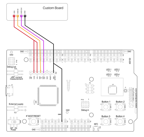
I'm trying to flash and debug an nrf52832 on an external board using an nrf52 dk. I have set up my wiring from P20 to a tag-connect TC2030 6-pin needle based on this diagram:
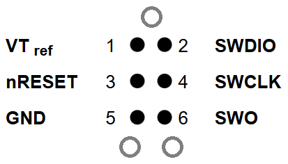
and assuming that the 6 connectors on the external board are laid out in the following way (viewed from above the board):
I've tried a variant where the external board gets its own power at 3v and that didn't work. I've been trying the option where the external board gets its power from the dev kit, however neither setup is working for me.
Here are some pictures of my wiring. Note that in this setup I'm also using the reset connection but with or without that connection I haven't been able to get it to work:
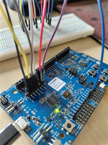
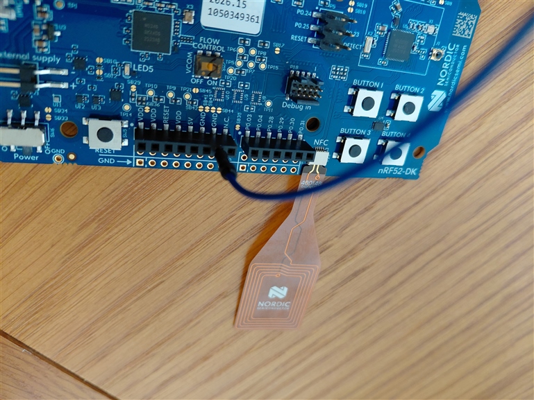
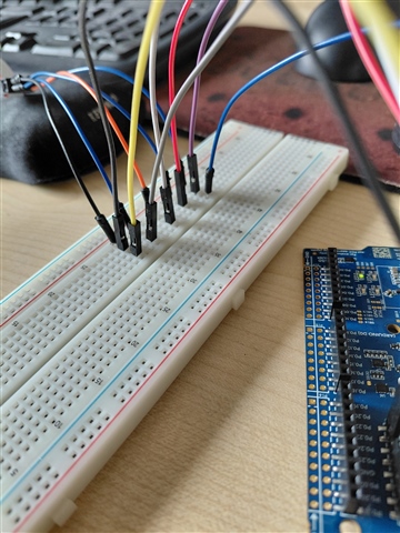
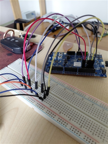
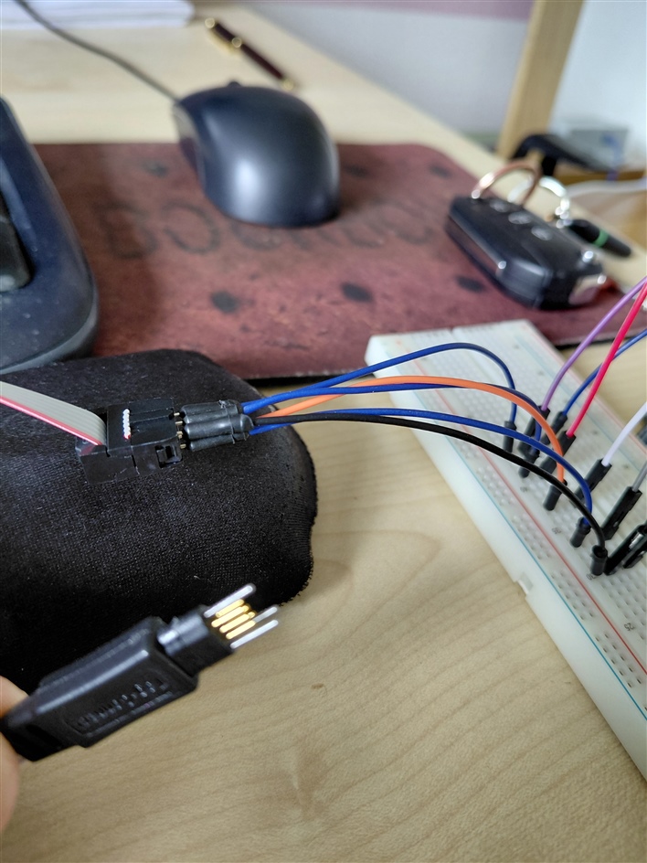
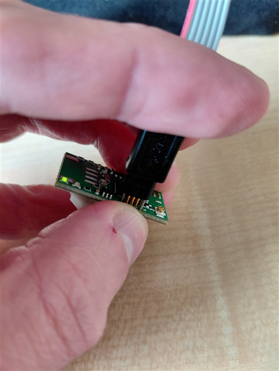
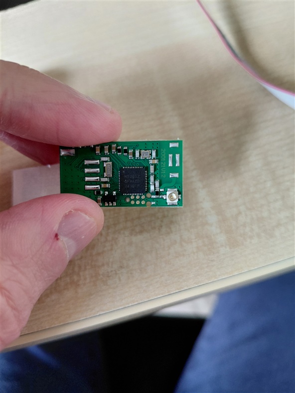
I've used a multimeter to confirm that the 6-pin needle pins have connectivity to the header via the correct routes. I.e. SWDIO -> SWDIO, SWDCLK -> SWDCLK etc..
I've also confirmed that my 6-pin needle is outputing a steady 2.98v between VDD and GND. When I attach the 6-pin needle my external board lights up and I have a flashing LED so I know it's getting power from the needle.
After some failures, I updated J-Link to the latest version 9.68a and I've updated my nrf52 dev kit to the latest firmware, but still no luck.
I believe the connection between my PC and the dev kit is fine as I've been able to flash and debug with it without any problems for the last few days and if I remove my wiring, it still works fine.
Here's the read-out from J-Link Commander when I try to connect to the external board:
SEGGER J-Link Commander V9.68a (Compiled Aug 17 2026 13:54:36)
DLL version V9.68a, compiled Aug 17 2026 13:53:37
Connecting to J-Link ...O.K.
Firmware: J-Link OB-nRF5340-NordicSemi compiled Jun 11 2026 13:12:28
Hardware version: V1.00
J-Link uptime (since boot): 0d 00h 00m 09s
S/N: 1050349361
License(s): RDI,FlashBP,FlashDL,JFlash,GDB
USB speed mode: Full speed (12 MBit/s)
VTref=3.300V
Type "connect" to establish a target connection, '?' for help
J-Link>connect
Please specify device / core. <Default>: NRF52832_XXAA
Type '?' for selection dialog
Device>
Please specify target interface:
J) JTAG (Default)
S) SWD
T) cJTAG
TIF>S
Specify target interface speed [kHz]. <Default>: 4000 kHz
Speed>
Device "NRF52832_XXAA" selected.
Connecting to target via SWD
InitTarget() start
InitTarget() end - Took 107ms
Failed to attach to CPU. Trying connect under reset.
InitTarget() start
InitTarget() end - Took 110ms
Error occurred: Could not connect to the target device.
For troubleshooting steps visit: kb.segger.com/J-Link_Troubleshooting
Does anyone have any ideas of what I could try next or can spot a problem in my setup?
Any help would be massively appreciated
Thanks
Mike
