This post is older than 2 years and might not be relevant anymore
More Info: Consider searching for newer posts

PCB design layout review

Hi

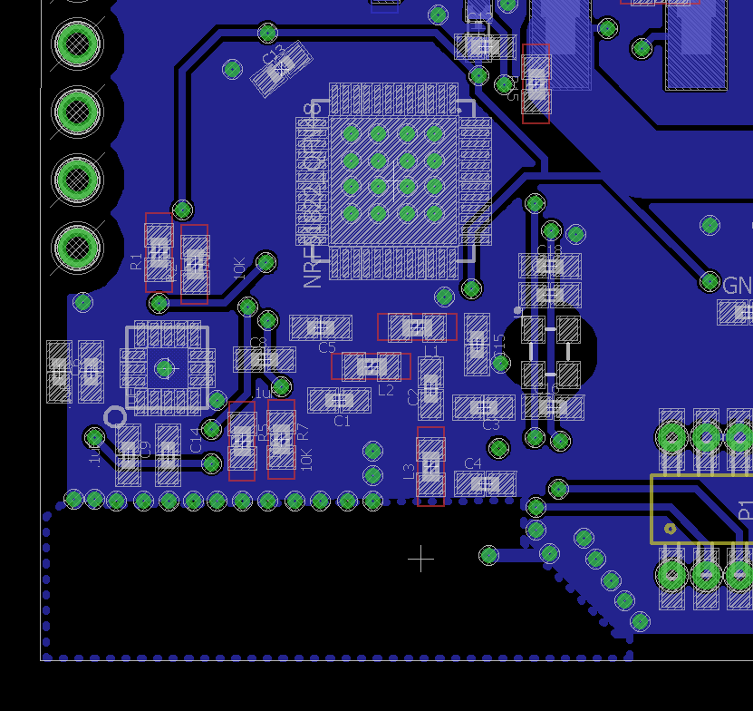
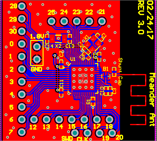
I'm using nrf51822 & PCB antenna due to size constraint I changed antenna direction (edit library file) so that it will fit within size. Also, components placement slightly different as recommended.

Please review my design

Here are top & bottom layer

Top Layer Bottom Layer

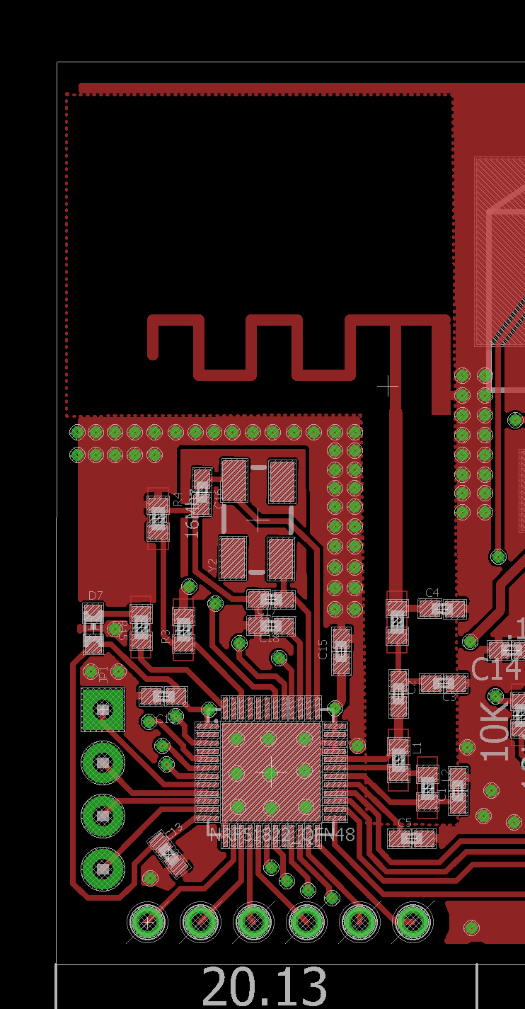
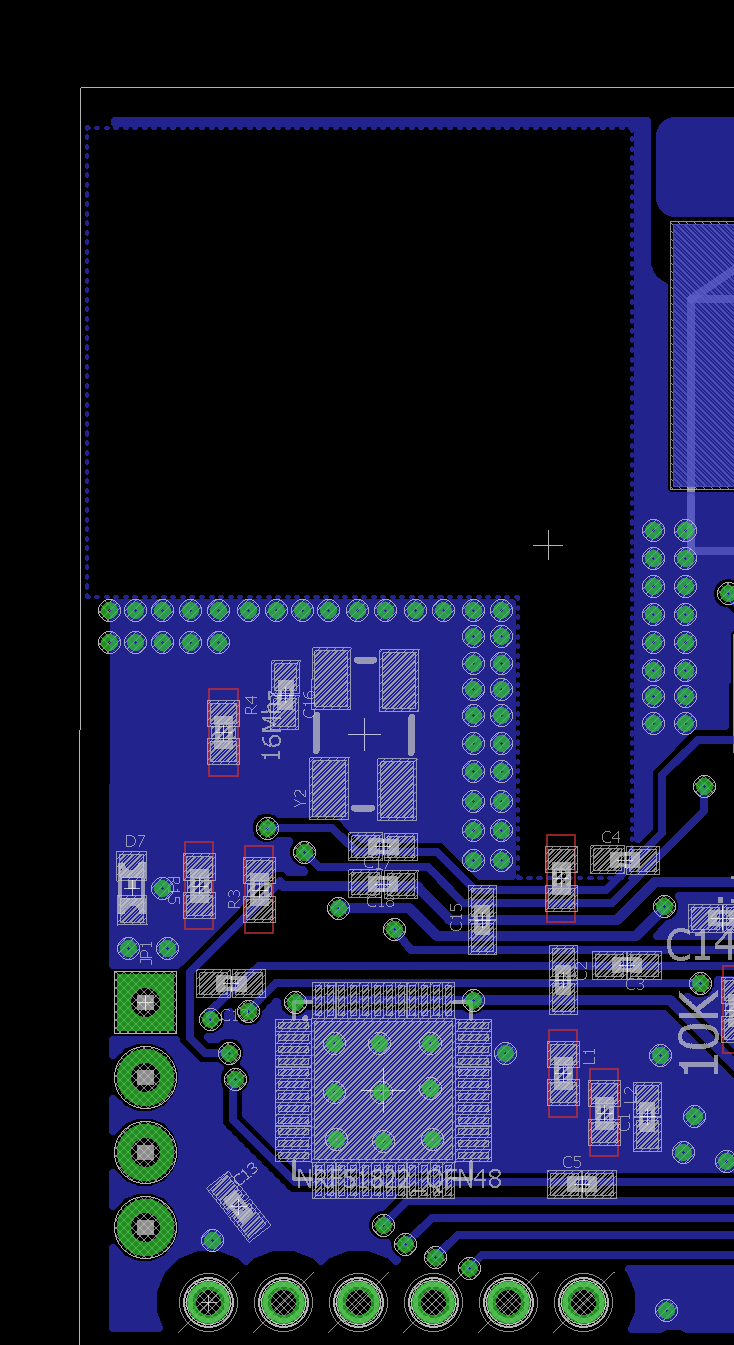
edit: I'm attaching updated layout

top

image description

  • There are several issues with this layout.

    1. The feed to the antenna is not characterized, nor is the connection for the match/lumped element balun. These all need to be characterized paths.

    2. Your RF traces seem to run over logic traces. This is not good practice and further illustrates how these are not characterized traces.

    3. Your crystal seems too large. The standard crystal Nordic likes to spec is only 2x1.6mm. Looks like you are causing layout issues just because of the large crystal. In addition most of the chip stuff looks like 0603 whereas you would save a lot of board space by placing 0402 or 0201.

    4. You would simplify the RF routing by rotating the nRF 90 CCW. Though a bigger problem is the ground plane for the inverted F meander hybrid does not look correct. Normally this type of antenna sits at the edge of the ground plane and not in a corner.

    5. I would suggest you consider the 52832 over the 51822. The 52832 has a single ended RF output that would simplify your layout a bit.

    Take a look at this layout. This person eventually ended up with a decent layout for 51822 using chip balun and meander antenna: image description

    Here is the blog entry for it: devzone.nordicsemi.com/.../

  • Here is a link to a Ti reference design for a meander inverted F hybrid. It shows the correct orientation of the ground plane for this type of antenna. www.ti.com/.../swra117d.pdf

  • Thanks

    Now I'm updated my layout, Please have a look

  • Both the 51822 and 52832 in QFN48 are 6x6mm. So no real space savings with 51822.

    With regard to the layout, much improved. Though you shouldn't ground the stub tuner on the F the way you did. Move C4 180 degrees to the left side of the feed and then you can terminate the stub on the F on the top plane where C4 used to be.

    You should also remove as much of that extra ground on the right side as you can. The bit next to the F. If you want keep a little so the antenna doesn't couple too much to your logic. So keep about 20mil and then stitch it.

    Also you don't need to stitch the ground as tightly as you do. Half as many vias would be fine. The way you did it would cause a dfm problem since the pcb gets weak in that area. Plus in terms of RF, half as many vias is just fine at 2.4GHz.

  • I should also point out you NEVER should do a shunt on a microstrip the way you did. You always place them on the strip not off to one side. When you place off one side the remaining bit of trace detunes the microstrip. Also, it changes the effect of the shunt device. So always place the shunts on the the microstrip.

    If you are determined to stay with the 51822, you should consider the chip balun/match as in the design I pasted into my comment. The chip balun will take up a fraction of the space of your lumped element balun and will have better harmonic rejection. Then maybe leave a series and a shunt after the balun to tune the antenna.

Related