
Hello,
In the reference layout for NRF52840 package (QIAA), the shape defined in the SOLDER PASTE is a bit larger than the one defined on TOP LAYER (copper) for each terminal pad. Is it normal and what's the point of it ?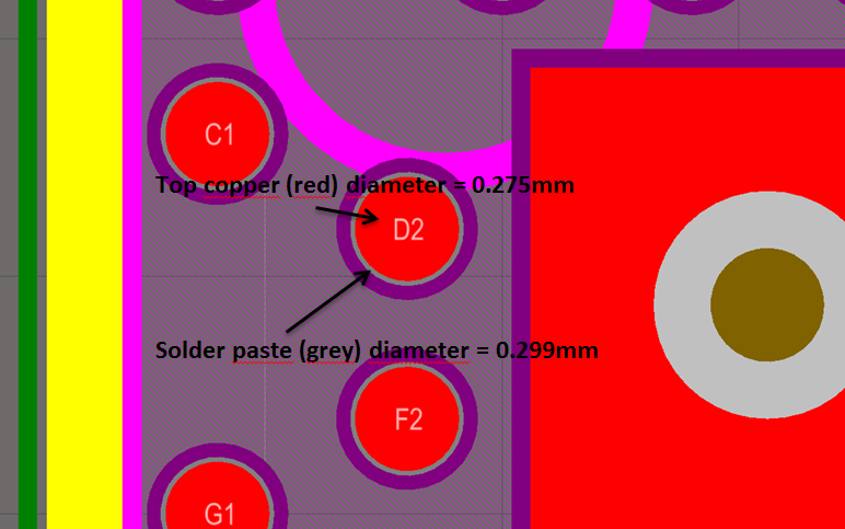
Hello,
In the reference layout for NRF52840 package (QIAA), the shape defined in the SOLDER PASTE is a bit larger than the one defined on TOP LAYER (copper) for each terminal pad. Is it normal and what's the point of it ?
