This post is older than 2 years and might not be relevant anymore
More Info: Consider searching for newer posts

PCB antenna design problem: too short range?

Dear Nordic,

Some time ago we started a project in which we decided to use ANT protocol to communicate wirelessly. However, now that we are going to production in a very very short time, we have spotted a very critical problem in the range of the communication.

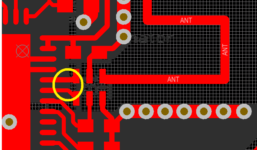
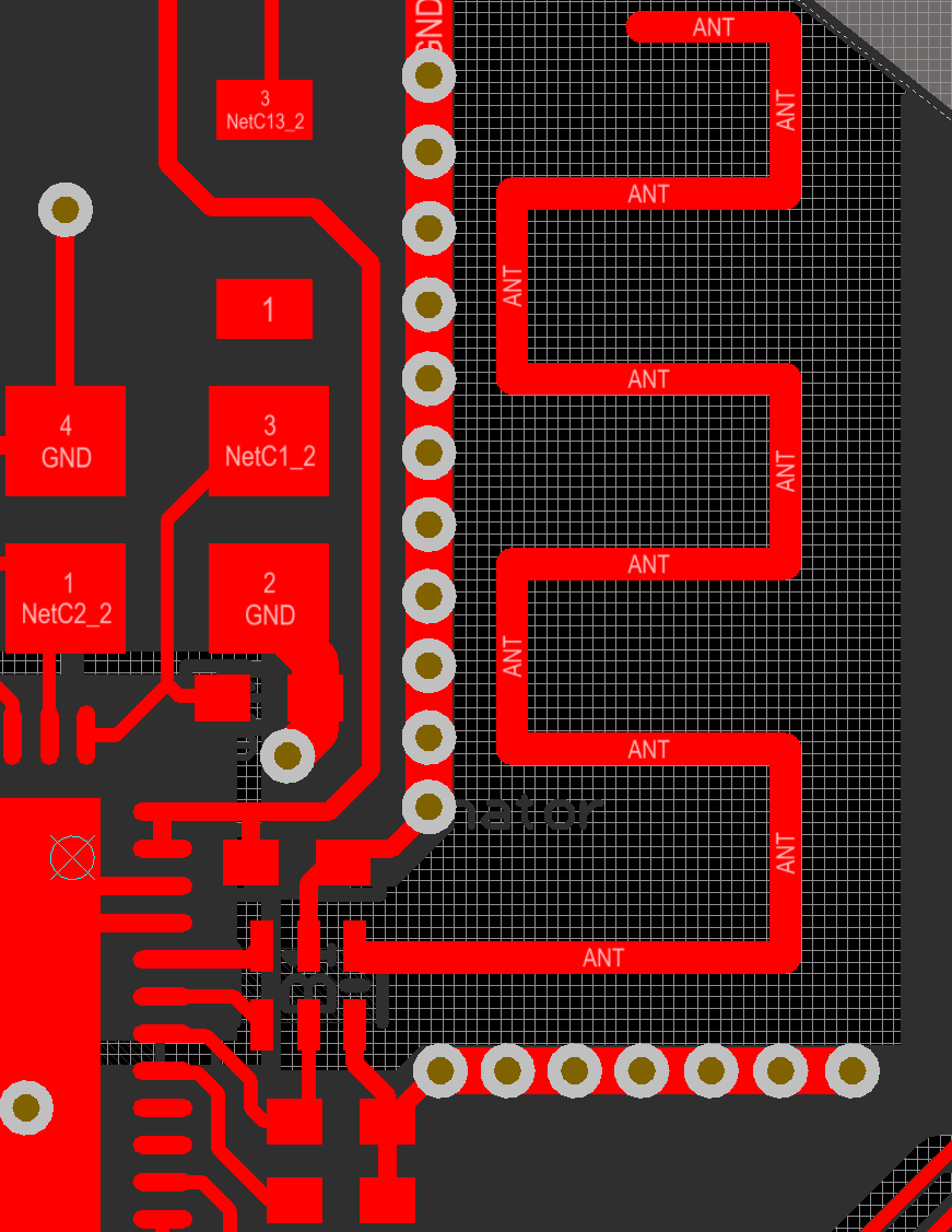
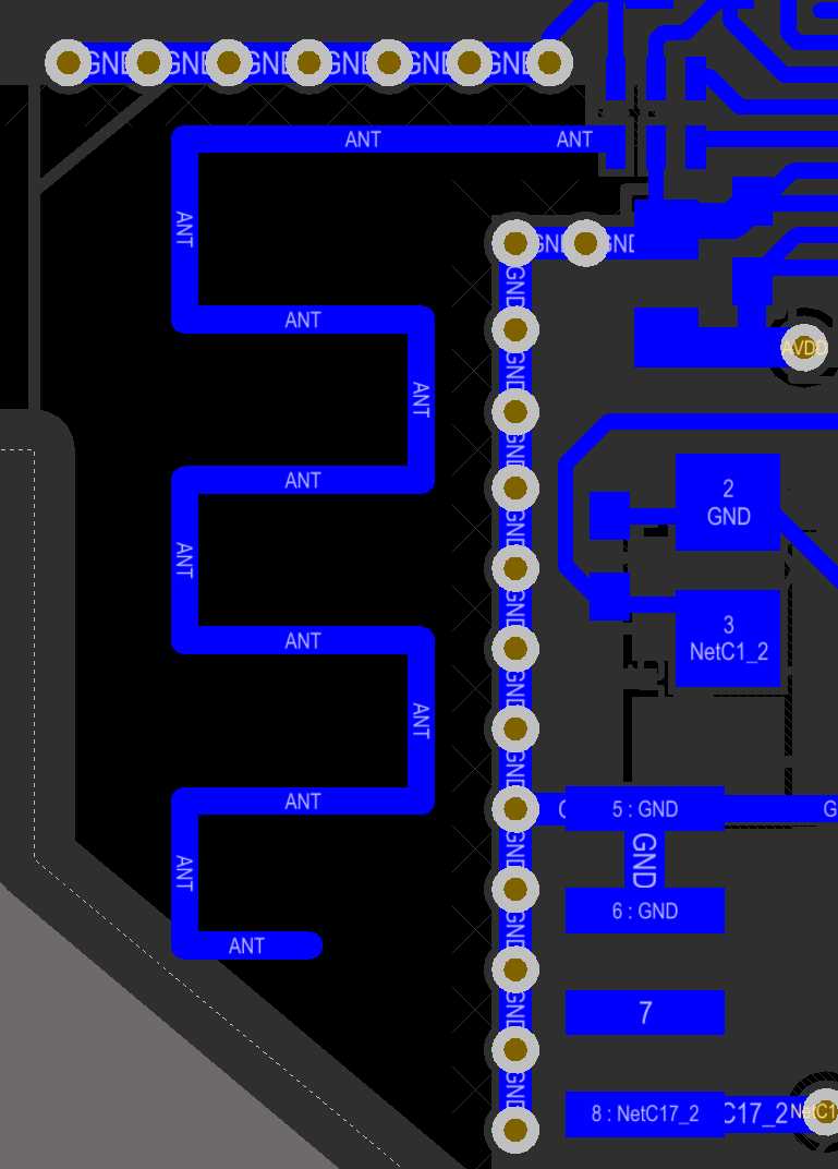
Here is the design of the antennas, in emitter and receiver pcb designs:

image description

image description

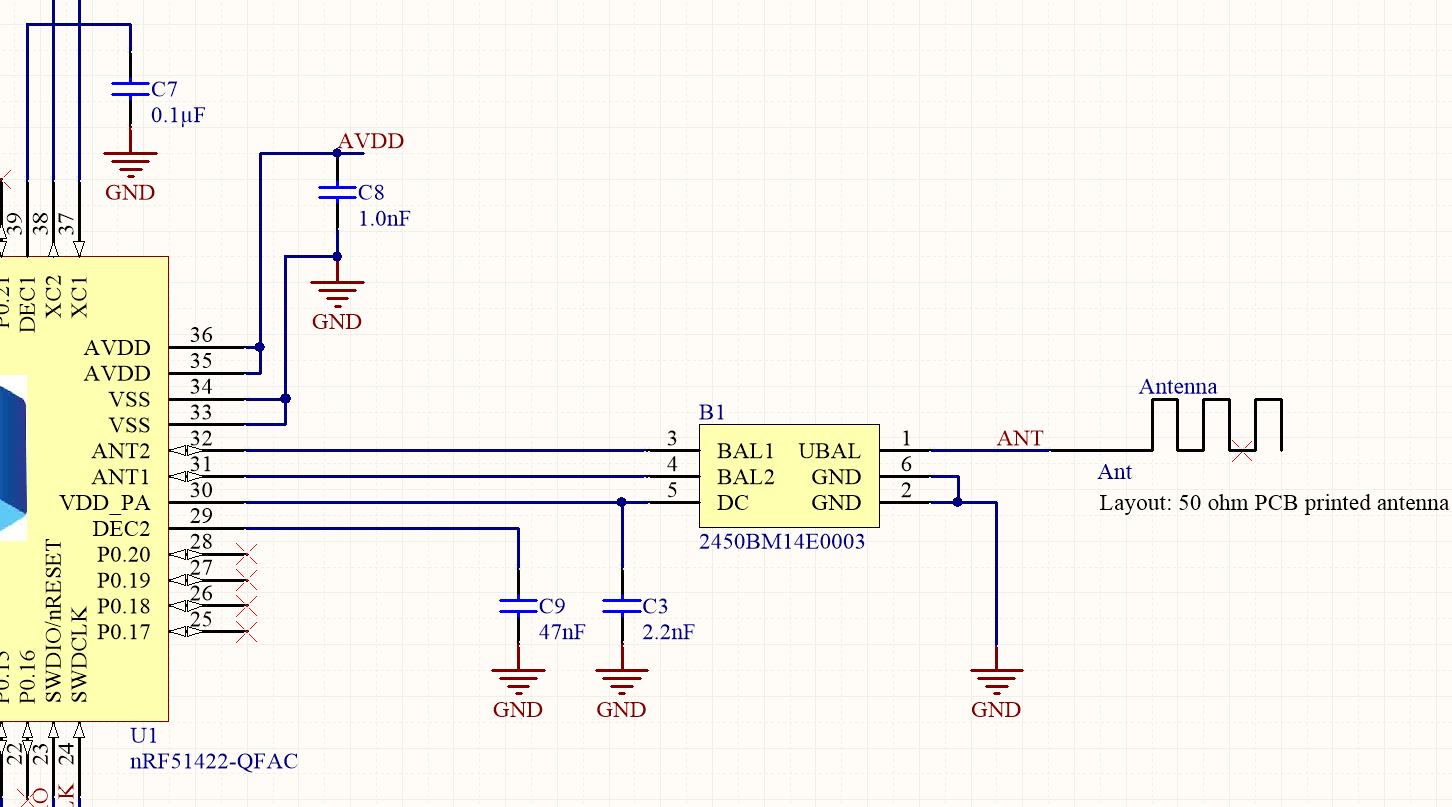
And here is the schematic for both of them:

image description

The total length of the antenna is 28.13 mm and the width 0.35 mm.

The main problem is that we only have like 1 to 1.5 meters of acceptable range. If I use the nordic DK as TX end, the range is significantly bigger, like 4 to 5 meters. This would be enough for our application.

Also, it is important to state again that the PCBs are already in production, so a solution requiring minimum changes in hardware would be better.

We have already tried different frequency numbers by SW (from 2400 MHz to 2524 MHz), but that only helped a bit (2433 MHz) seems to work a bit better.

Also changed the RADIO_TX_POWER to +4dBm but didn't really do anything.

Anyone has any idea how we could improve the range of our antenna? Again, I know that the same software using the DKs has a really good performance.

Thank you very much for your help.

Parents
  • Hi, Angel. I think there is a minor issue with the ANT1 (31) and ANT2 (32) pin.

    it is important to state again that the PCBs are already in production, so a solution requiring minimum changes in hardware would be better.

    Hmm, I hope for your understanding that my answer won't be a big help.

    While waiting for a better solution / answer provided by the Nordic's dev-team, take a look at my answer, please.

    This issue was detected from the Nordic's distributor when I was creating a custom PCB that uses nRF52832.

    Take a look of the PCB traces of pin 31 and 32, please.

    ref. Nordic devzone - PCB Antenna. Tuning not necesary

    BalunExample

    ref. Nordic Blog - General PCB design guidelines for nRF51

    image description

    Both traces are symmetric; they are stretched with the same length and bent at the same y position.

    As a result, the balun's center is aligned to the center of pin 31 and 32.

    Also, as you see the blog's picture, there are plenty of ground vias at the nRF51 MCU footprint.

    Whereas,

    Yours

    your trace is not symmetric. The trace of pin 31; it is bent "earlier".

    So the balun's center is not aligned.

    Also, I can't tell whether your PCB has sufficient ground vias at the nRF51 MCU footprint.

    This type of issue has an effect on matching network.

    Like "Dave" 's comment, have you used an impedance calculator?

    Also, how is the ground pour configured below the matching network?

    -Best Regards

Reply
  • Hi, Angel. I think there is a minor issue with the ANT1 (31) and ANT2 (32) pin.

    it is important to state again that the PCBs are already in production, so a solution requiring minimum changes in hardware would be better.

    Hmm, I hope for your understanding that my answer won't be a big help.

    While waiting for a better solution / answer provided by the Nordic's dev-team, take a look at my answer, please.

    This issue was detected from the Nordic's distributor when I was creating a custom PCB that uses nRF52832.

    Take a look of the PCB traces of pin 31 and 32, please.

    ref. Nordic devzone - PCB Antenna. Tuning not necesary

    BalunExample

    ref. Nordic Blog - General PCB design guidelines for nRF51

    image description

    Both traces are symmetric; they are stretched with the same length and bent at the same y position.

    As a result, the balun's center is aligned to the center of pin 31 and 32.

    Also, as you see the blog's picture, there are plenty of ground vias at the nRF51 MCU footprint.

    Whereas,

    Yours

    your trace is not symmetric. The trace of pin 31; it is bent "earlier".

    So the balun's center is not aligned.

    Also, I can't tell whether your PCB has sufficient ground vias at the nRF51 MCU footprint.

    This type of issue has an effect on matching network.

    Like "Dave" 's comment, have you used an impedance calculator?

    Also, how is the ground pour configured below the matching network?

    -Best Regards

Children
  • Hi MANGO,

    First of all, every answer is of very good help, thank you very much for your reply!

    I see that you in the thread that you link, in the end, the decision of removing the Pi network is taken. We also have no laboratory equipment available to do these tuning measurements, so I assume that for us is also useless to put a pi network there.

    As I wrote as a reply to my previous question, there is a ground plane right below the antennas, that is connected through these lanes that you see next to the antenna. Do you think that it is enough grounding?

    About the centering of the Balun, do you think it will affect a lot if we align it? I mean, can it affect significantly to the range of the antenna?

    Thanks again for your reply!

    • Best
  • Hello, Angel. As mentioned, these (aligning the balun) are minor issues.

    I was informed from the Nordic's distributor, so I don't know the exact math about this.

    It will affect the antenna range, but it will be minor, compared to the effect due to the ground plane which is beneath the antenna.

    I created a custom 4-layered PCB that used nRF52 and λ/4 printed monopole antenna.

    This one had the above minor issue; I accidentally created a non-symmetric trace.

    Using the DTM mode, the TX power from 2.4GHz (actually recorded 2.399987GHz) was -0.7dBm.

    So you can speculate that this doesn't affect much.

  • About there is a ground plane right below the antennas, Do you think that it is enough grounding?

    Well, as far as I know, as mentioned in here, There shall be no ground plane on the PCB layer(s) beneath the antenna trace. No ground plane, PCB traces or components should be placed close to the antenna trace.

    I think there was a confusion about Do you think that it is enough grounding?

    The grounding was about top / bottom ground pour. However, that ground plane has to be kept out below the antenna.

    So Jørn was asking that In other words, have you maintained a keep-out region on all layers underneath the antenna?

    Can you upload the details about your PCB so that we can check the ground plane?

    -Best Regards

  • Adding a Pi-Network is critical to almost every RF design. The Balun only matches between the balun itself and the nRF chip, but like a transformer it needs an impedance matched load. Have you used a Network Analyzer to measure the matching of your Antenna?

    More than likely, the unbalanced tracing to the balun, along with the un-tuned trace and antenna means you're getting high RF reflections on the board thats drastically affect your Transmitted RF.

Related