Hi everybody,
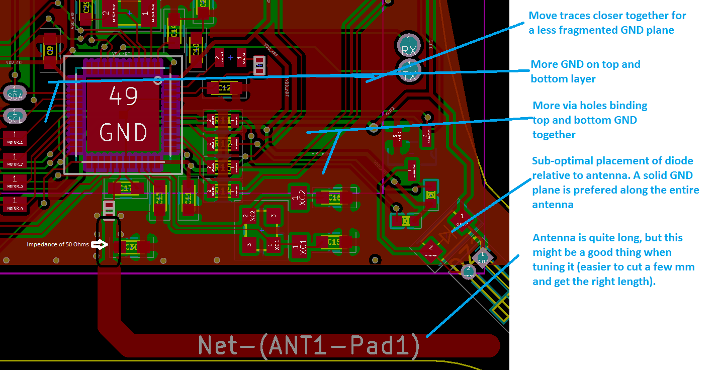
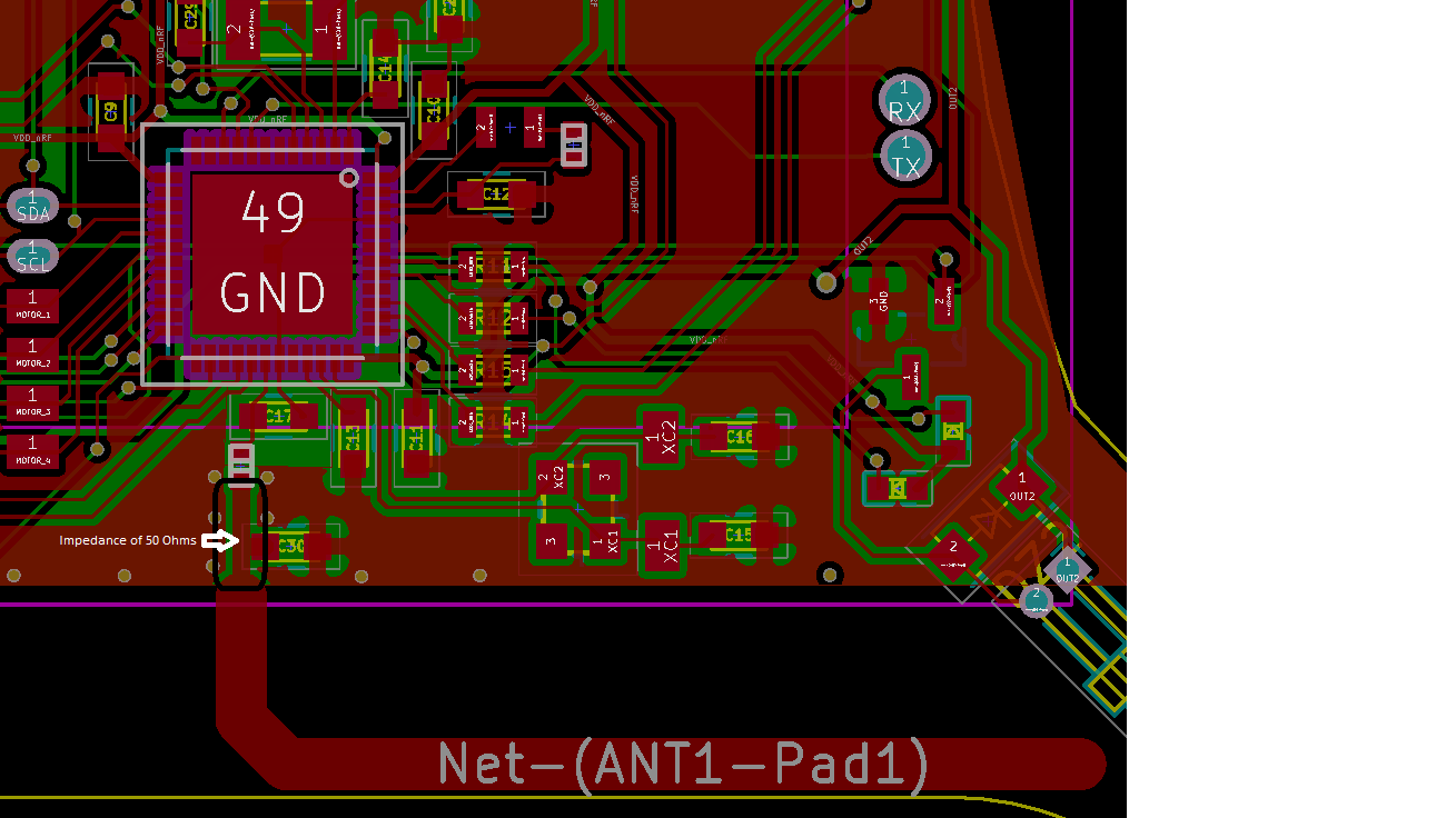
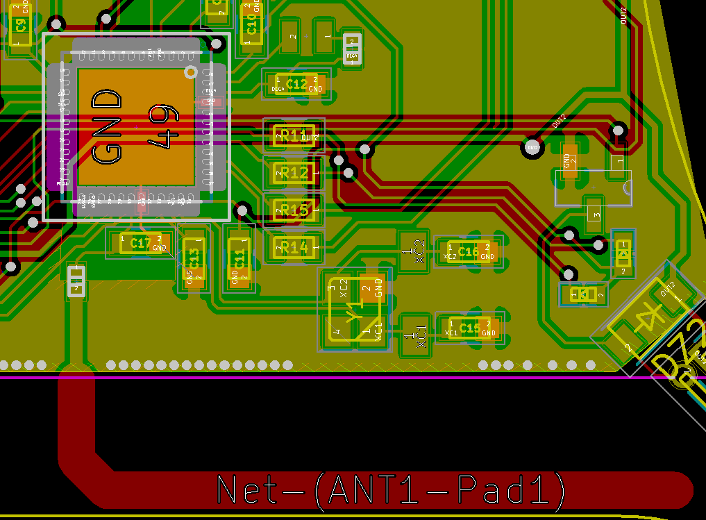
I have an issue with my application, I want to use the ble with the same antenna that it use in the development board PCA10036, Could you please tell me if the matching and the circuit for antenna is correct ?
Thank you for your help,
Hi everybody,
I have an issue with my application, I want to use the ble with the same antenna that it use in the development board PCA10036, Could you please tell me if the matching and the circuit for antenna is correct ?
Thank you for your help,