Hi everybody,
I have an issue with my application, I want to use the ble with the same antenna that it use in the development board PCA10036, Could you please tell me if the matching and the circuit for antenna is correct ?
Thank you for your help,
Hi everybody,
I have an issue with my application, I want to use the ble with the same antenna that it use in the development board PCA10036, Could you please tell me if the matching and the circuit for antenna is correct ?
Thank you for your help,
We always recommend following our reference schematic and layouts found here.
Here is another good PCB layout guideline.
Here you can also find the PCA10040 hardware files. Take a look and try to copy the matching network as well as the antenna.
EDIT: Continued:
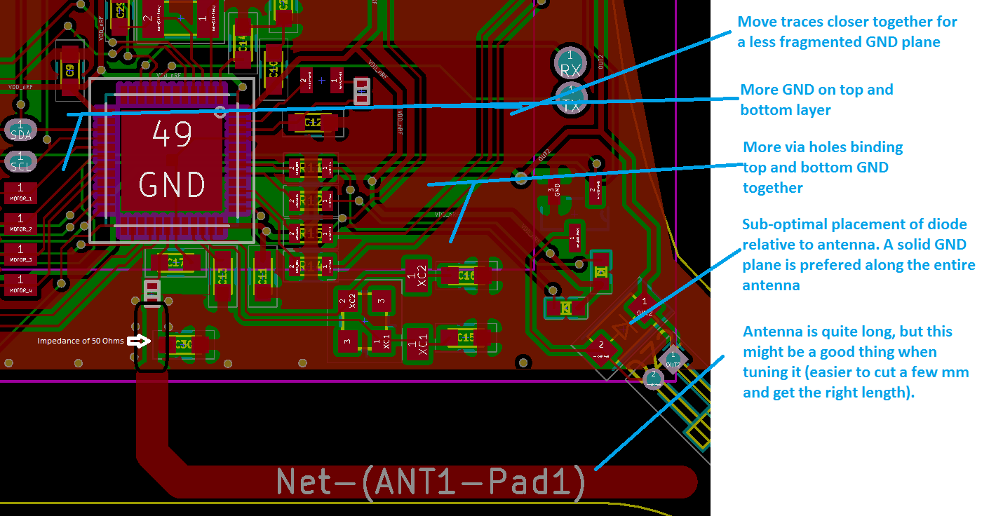
Your changes look much better. Here are some more suggestions though:

In general you can't get too much grounding so try to clean up the traces a bit and pour some ground into the large empty spaces. Also try to use lots of vias on your entire PCB, not just around the antenna, to tie the top and bottom GND together. You should also have a large solid ground plane below the matching network.
We always recommend following our reference schematic and layouts found here.
Here is another good PCB layout guideline.
Here you can also find the PCA10040 hardware files. Take a look and try to copy the matching network as well as the antenna.
EDIT: Continued:
Your changes look much better. Here are some more suggestions though:

In general you can't get too much grounding so try to clean up the traces a bit and pour some ground into the large empty spaces. Also try to use lots of vias on your entire PCB, not just around the antenna, to tie the top and bottom GND together. You should also have a large solid ground plane below the matching network.
I will use your tips to optimize my circuit, Thank you so much Martin for your help,
Best regards,
Omar
Happy to help!