This post is older than 2 years and might not be relevant anymore
More Info: Consider searching for newer posts

Suggestion for NRF52832 custom PCB

Hi,

I have designed a custom PCB using NRF52832 IC.I have followed Sparkfun NRF52832 breakout board for placement of NRF52832 IC core part(including antenna) which is similar to the recommended reference design in the datasheet. SparkFun board link: learn.sparkfun.com/.../nrf52832-breakout-board-hookup-guide

My board dimensions: 100x50 mm.

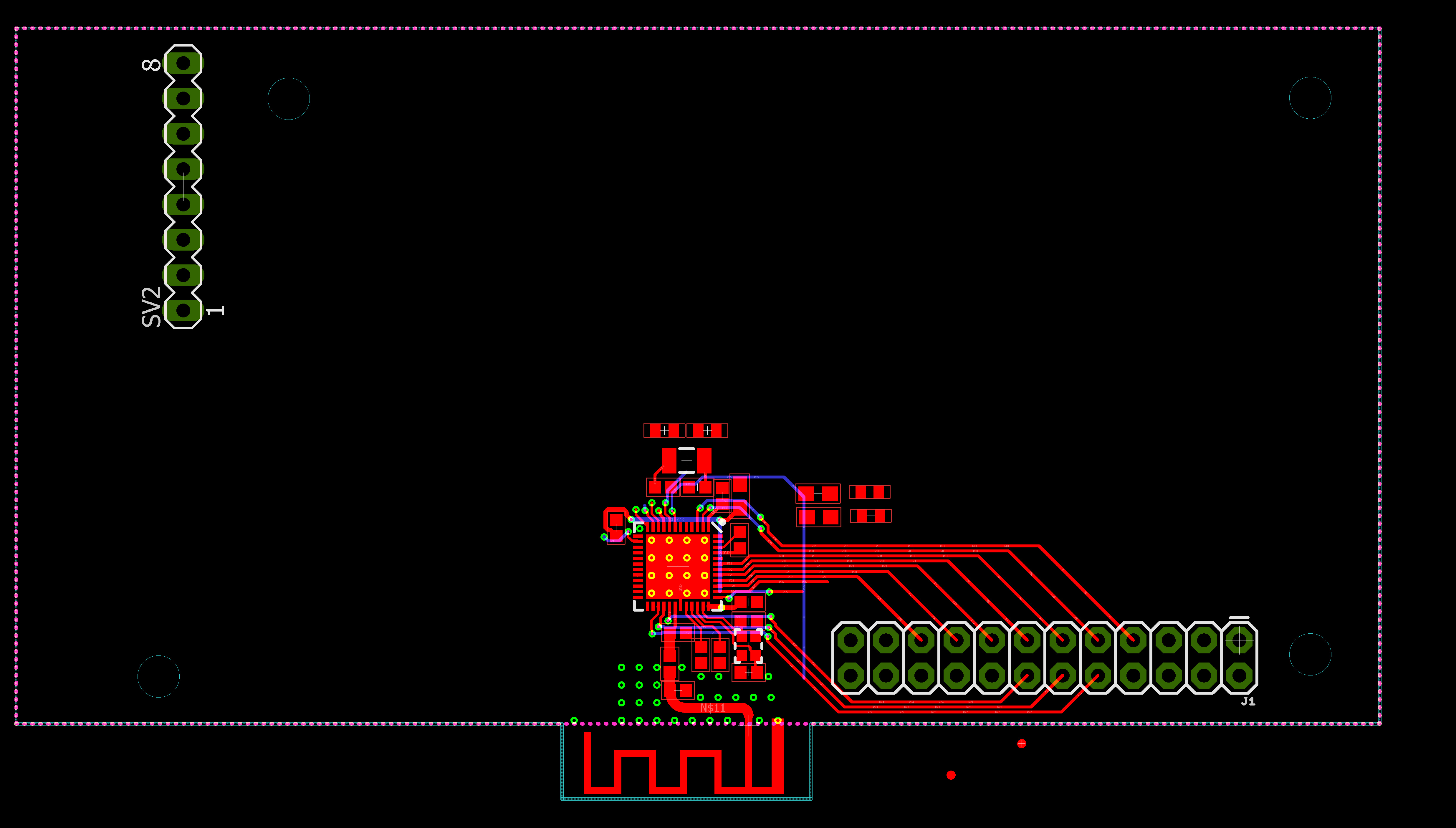
Is this design OK? Need improvements/suggestions for my design. image description.
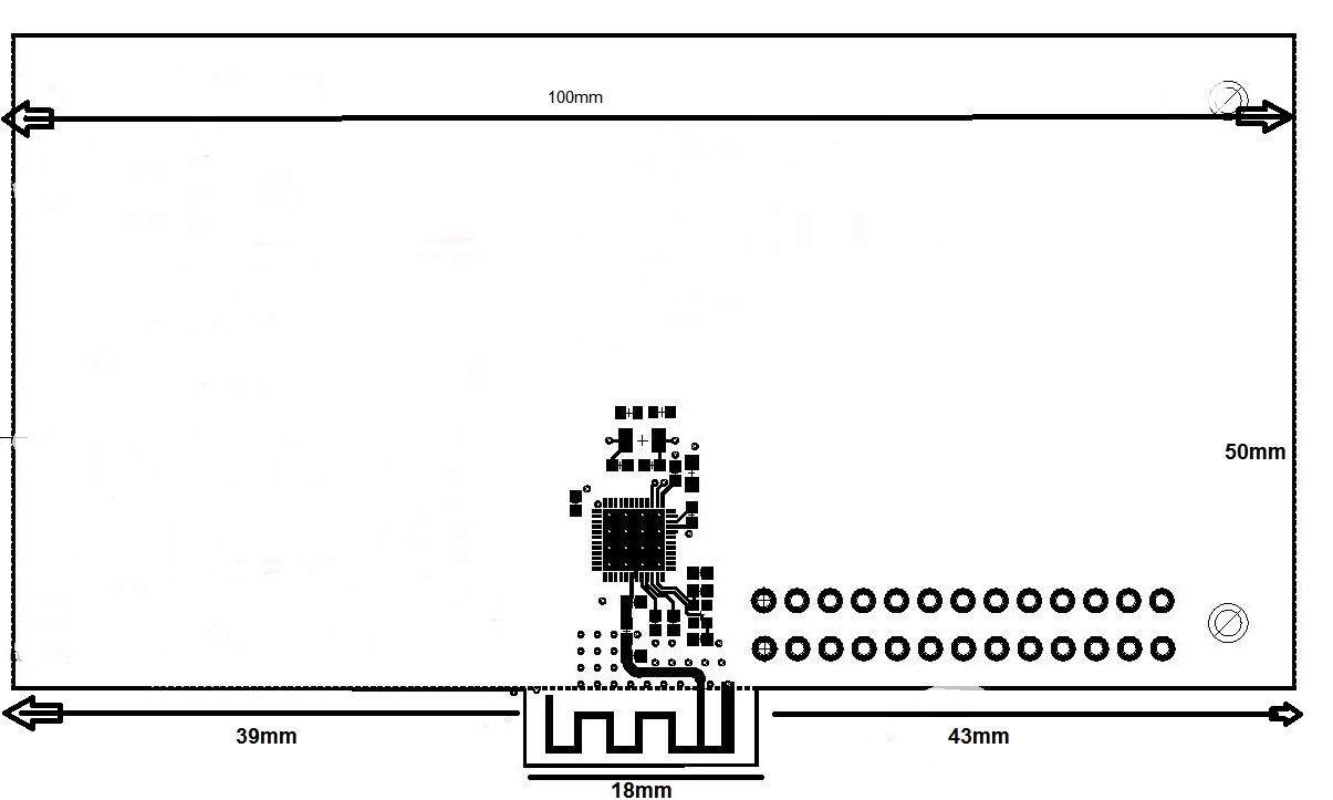
Layout:image description

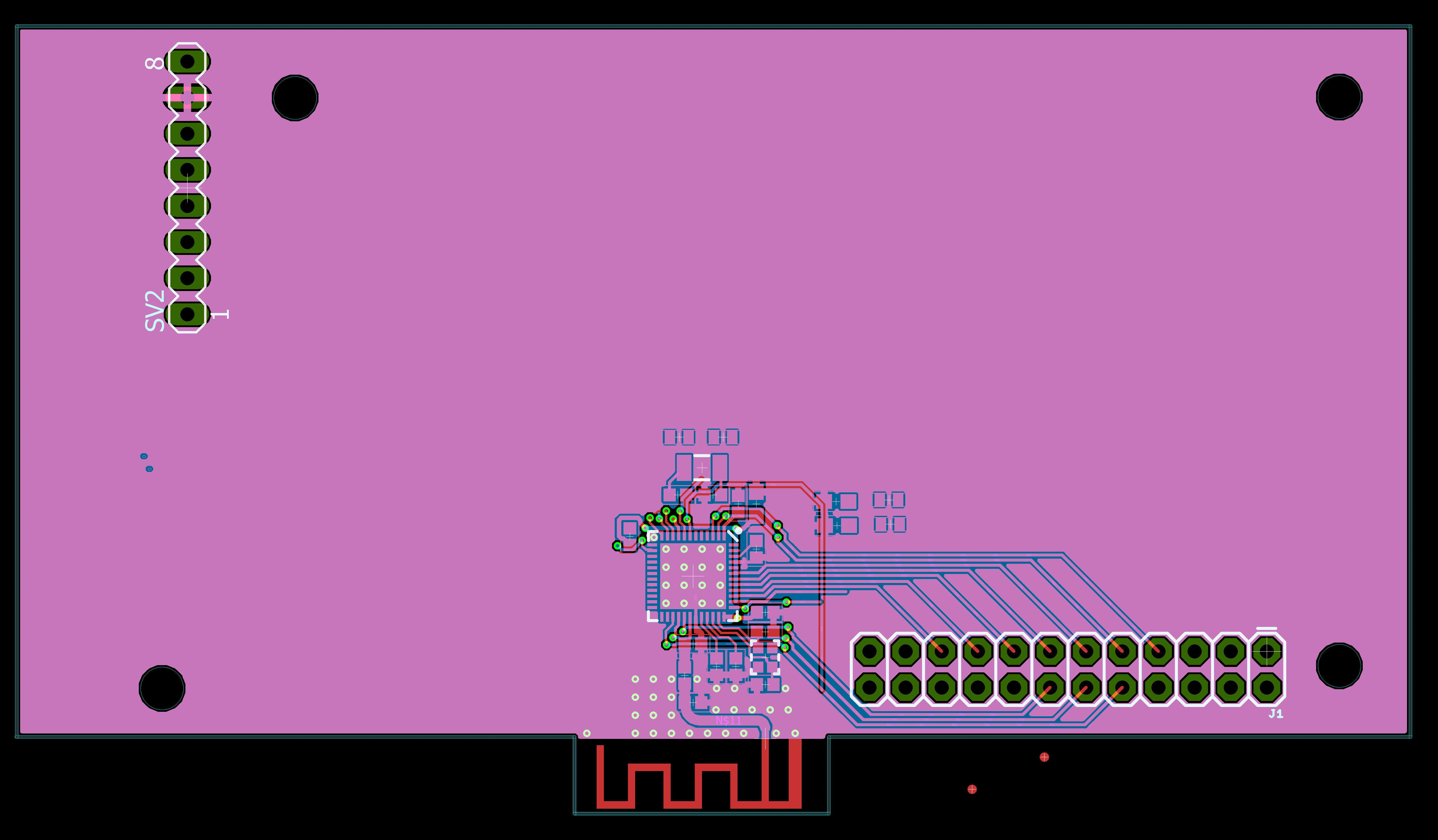
Ground planes: image description

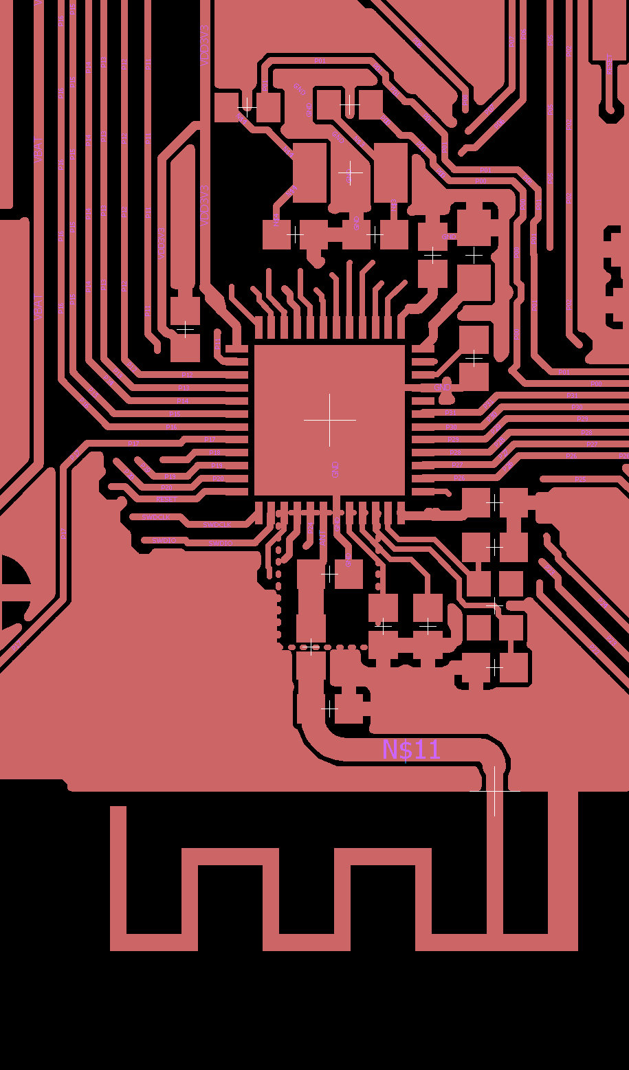
Layout after adding polygon cut-outs around matching circuit elements:image description
Parents
  • Reposting question to "jump" it up is not recommended here. If you don't hear from us you can send a private message either to the one handling your question or to other Nordic employees if you don't hear from him (in case he is travelling, on vacation).

    Regarding your design, I don't see the ground plane on the top layer, maybe it's hidden ? Seems like you haven't added the tuning components (if you don't have tool to tune the antenna and don't plan to send your prototype to us for tuning, then they are not needed). Note that for the mean antenna, it's harder to tune using just one shunt component compare to monopole pcb antenna.

    I assume you use the matching network component values from our reference design.

    I'm not sure why your board has to be that big. Is that to match with the SparkFun board ? What is that track running vertically on the right side of the chip ?

    We recommend to follow our reference design for nRF52 (you can find on our website). You can also have a look at the design of the nRF52 DK.

Reply
  • Reposting question to "jump" it up is not recommended here. If you don't hear from us you can send a private message either to the one handling your question or to other Nordic employees if you don't hear from him (in case he is travelling, on vacation).

    Regarding your design, I don't see the ground plane on the top layer, maybe it's hidden ? Seems like you haven't added the tuning components (if you don't have tool to tune the antenna and don't plan to send your prototype to us for tuning, then they are not needed). Note that for the mean antenna, it's harder to tune using just one shunt component compare to monopole pcb antenna.

    I assume you use the matching network component values from our reference design.

    I'm not sure why your board has to be that big. Is that to match with the SparkFun board ? What is that track running vertically on the right side of the chip ?

    We recommend to follow our reference design for nRF52 (you can find on our website). You can also have a look at the design of the nRF52 DK.

Children
No Data
Related