This post is older than 2 years and might not be relevant anymore
More Info: Consider searching for newer posts

nRF52832 IO problem

Hello!

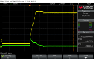
We have nRF52832 chip on our product and we have some problem with one of its IOs.. We configured P0.16 as RX of UART, And when we run it we see this behavior of this IO:

VCC (yellow) vs P0.16 (green) that configured as UART_RX

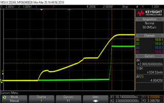
Here we see that with rising of VCC (yellow signal) IO (green) rising to almost 1V when it supposed to still at 0V. Important note: we disable and enable VCC fast here so we see that before rising of VCC it don't have 0V. This behaviour is very problematic to our system. Because we have power supply sensitive sensor that connected to this UART. This spike of voltage damage sensor that connected to this IO.

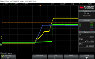
We tried to load to evaluation board same version of SW on nRF52832 and we got next result:

We see that also here we have the problematic spike.

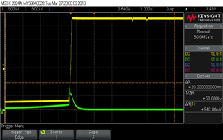
When we erased the evaluation board - we got the same result.

Is this IO known as problematic?

Thank you

Parents
  • It seems very curious that the sensor is getting damaged due to a spike that's <1V for just a small period of time.  

    For a typical UART configuration, the 'inactive' state will be HI and a transmission starts with the transition from HI-LOW, indicating the start bit when a byte is arriving.  Even after the little 'bump' on power-up (which seems very reasonable, it takes a small amount of time for the processor to get control of the IO), I would expect that the UART RX line would get pulled hi, especially with the 100k pull-up that you mention.  Something is strange here.    

    You also mention that your sensor is powered off of 9V.  I assume you're using some sort of level-shifter to make sure that any signals sent to the NRF are down at a safe voltage level, correct?

    Cheers,

    Roger

  • Yeah, it is also very strange for us also..

    The sensor powered by 9V, but it have on-sensor buck converter that convert 9V to 3.3V to power-up the on-sensor microprocessor MSP430G2744. This on-sensor microprocessor is the part that communicate via UART with nRF. The 9V used only for accelerometer that placed on the sensor.

    As I write this I am thinking about something - is this possible that on-sensor buck output come lately after the signals from nRF?.. Need to check this.

  • After some running. tests and tries we found that our sensor still get damaged.. We put series resistor of 500 ohm on our signal that needed to bring maximum 6.6 mA to the IO - the current that MSP supposed to hold on.. Now we are running tests with buffers..

  • Hello!

    We tried also to use buffer at this signal. But after 2 weeks the sensor also get damaged.. What can be te reason that the IO still get damage?

    Thank you

  • I think a schematic is required so I can see the power sources and (more importantly) the power sequencing. You may be seeing back-drive, phantom power or simple spike damage. If the schematics are confidential maybe provide some secure access or post to Nordic engineers privately (I am not Nordic, just a freelance designer)

  • Here it is: 

    Charger accept 5V Vbus or 3.7V nominal from Battery if Vbus no connected. After it - this voltage boosted to 9V for sensor and then 3.3V created.

    The waveforms for this power sequesting:

  • Deriving the 3.3V Buck from the 9V Boost is an unusual choice and is likely to be both inefficient and troublesome; if that choice was made for sequencing then it would be better handled by deriving both regulators from the charger with an alternative enable/disable method for sequencing. Focusing on the sensor can you show what happens to the 9V as I recall you posted the sensor was an MSP430 so the interesting part of the circuit is not shown; also I can't make out the inductor shown on the sensor, is that a feedthrough or a real inductor? It's difficult to see the connection.. the sensor schematic would clarify these questions.

Reply
  • Deriving the 3.3V Buck from the 9V Boost is an unusual choice and is likely to be both inefficient and troublesome; if that choice was made for sequencing then it would be better handled by deriving both regulators from the charger with an alternative enable/disable method for sequencing. Focusing on the sensor can you show what happens to the 9V as I recall you posted the sensor was an MSP430 so the interesting part of the circuit is not shown; also I can't make out the inductor shown on the sensor, is that a feedthrough or a real inductor? It's difficult to see the connection.. the sensor schematic would clarify these questions.

Children
Related