This post is older than 2 years and might not be relevant anymore
More Info: Consider searching for newer posts

range of custom pcb

Hi,

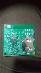
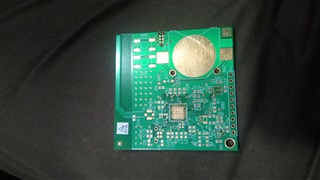
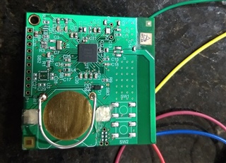
  My nrf 52840 pdk and my custom pcb with nrf 52840 soc. both are running with same application ble_proximity example from sdk 14.1 and softdevice s140 5.0. when i set the Tx_power to 4dbm. i am expecting the range of custom pcb should be equal to my pdk. but the range of custom pcb is very low when compared to pdk. how can i achieve the range of custom board equal to pdk?

thanks and regards,

karthikeyan

Parents Reply Children
  • hi,

      there was little bit problem in distance. how to achieve that?

    thanks and regards,

    karthikeyan

  • Well, I'm still not convinced you have your antenna hooked up correctly.  It would be nice to see a photo of it correctly hooked up and J1 bypass as you have indicated was completed.

    But assuming J1 has been bypassed correctly then your range issues are then a function of impedance matching. They can only be resolved with a VNA and someone who knows how to use it.

  • hi,

      i have uploaded the image of pcb before assembly of the components. in that J1 as not scratched.

  • We are still not communicating correctly. I wanted to see a photo of your board after you fixed your problem with J1.

    What I can see from the photo above it looks like you used the mostly correct artwork for the micro coax test port. But what you did wrong is that you placed the wrong connector for J1 instead of a micro coax test port.

    To fix this problem you can either buy the correct microcoax test port and place it.  Or, you can bypass the input and output with a chip cap or small piece of wire.  You do not and should not scratch any ground away. That is unnecessary and will keep the micro coax test port from working if you ever buy it.

    On your next spin, one thing you should fix is that the ground plane under J1 should be solid and not connected via small traces.  This ground plane is important for the connector to work correctly. Similarly the ground pads for the connector should not have thermals.  It should connect connect solidly to the surrounding ground and vias should be placed close to or even in the ground pad.

    For reference here is the correct artwork for the testport from the DK pcb:

    Please note the two vias inside of the ground pad.  These are very important. Simply placing them off to one side as you did is not sufficient. Also note, NO THERMALS!!!

    If you don't ever intend to use the testport, and many people have no need for it, you can just bypass it in the artwork.  Here is a devzone question about that: https://devzone.nordicsemi.com/f/nordic-q-a/35133/pcb-antenna-nrf52810-eagle-files-does-it-need-extra-components-for-impedance-matching

    For your reference this is how you bypass J1.  Normally this can be accomplished with a 1206 or 0805 part.:

  • I'm developing custom board using nrf52840.

    Previously my ex-colleague was developing the board and now I'm taking care of this, so it would be helpful if you could assist me on completing the board.

    At present, the board is almost complete and I would need to check the design is correct as per guidelines.

    case ID: 207780 - This is the case ID used by the previous developer.

    I have attached below the image of the custom board,

    Can you please check the board and suggest me if this is correct ?

Related