This post is older than 2 years and might not be relevant anymore
More Info: Consider searching for newer posts

nrfjprog can't read/write/erase correctly nrf52840 MX25R6435F QSPI

Greetings!

Using the NRF52840 PDK, I succesfully erase, write and read without any modifications!

I have custom boards which involved a NRF52840 and a MX25R6435F (so same setup as the PDK), I just made modifications on the QspiDefault.ini since my pinout is different.

I try to erase all the flash chip or just one page but nrfjprog doesn't returned me any errors (so success ?) but it has no effects since I can read the chip which gives me 999999999999....9

I also try the --qspicustominit, different write and read mode but no changes.

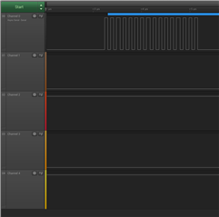
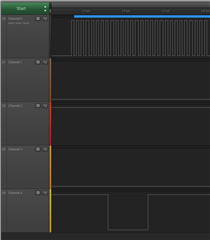
(Assuming the wires are correctly solde ); channel 0 is clock, channel 1 is DIO0, channel 2 is DIO1 ...

This is the result for running a read of 8 bytes:

Thanks for your time.

  • Hi,

    Are you able to program the board using nrfjprog?

    Could you provide the log file from nrfjprog (add the parameter --log and provide file log.log)? Please also upload scematics for your board.

    Best regards,
    Jørgen

  • Thanks for your reply,

    Yes I can program the board, moreover I have a working QSPI driver (so the connection isn't involved)

    Here's in the log file for nrfjprog --memrd 0x12000000 --log

    --------------------------------------------------------------------------------
    nrfjprog --memrd 0x12000000 --log
    nrfjprog verion 9.7.2
    --------------------------------------------------------------------------------
    FUNCTION: open_dll.
    FUNCTION: open_dll.
    FUNCTION: enum_emu_snr.
    FUNCTION: enum_emu_snr.
    FUNCTION: enum_emu_snr.
    FUNCTION: enum_emu_snr.
    FUNCTION: connect_to_emu_with_snr.
    FUNCTION: connect_to_emu_with_snr.
    FUNCTION: connect_to_emu_without_snr.
    FUNCTION: enum_emu_snr.
    Device "NRF52832_XXAA" selected.
    FUNCTION: read_device_version.
    FUNCTION: read_device_version.
    Found SW-DP with ID 0x2BA01477
    Found SW-DP with ID 0x2BA01477
    Scanning AP map to find all available APs
    AP[2]: Stopped AP scan as end of AP map has been reached
    AP[0]: AHB-AP (IDR: 0x24770011)
    AP[1]: JTAG-AP (IDR: 0x02880000)
    Iterating through AP map to find AHB-AP to use
    AP[0]: Core found
    AP[0]: AHB-AP ROM base: 0xE00FF000
    CPUID register: 0x410FC241. Implementer code: 0x41 (ARM)
    Found Cortex-M4 r0p1, Little endian.
    FPUnit: 6 code (BP) slots and 2 literal slots
    CoreSight components:
    ROMTbl[0] @ E00FF000
    ROMTbl[0][0]: E000E000, CID: B105E00D, PID: 000BB00C SCS-M7
    ROMTbl[0][1]: E0001000, CID: B105E00D, PID: 003BB002 DWT
    ROMTbl[0][2]: E0002000, CID: B105E00D, PID: 002BB003 FPB
    ROMTbl[0][3]: E0000000, CID: B105E00D, PID: 003BB001 ITM
    ROMTbl[0][4]: E0040000, CID: B105900D, PID: 000BB9A1 TPIU
    ROMTbl[0][5]: E0041000, CID: B105900D, PID: 000BB925 ETM
    FUNCTION: qspi_init.
    FUNCTION: qspi_init.
    FUNCTION: qspi_read.
    FUNCTION: qspi_read.
    FUNCTION: qspi_uninit.
    FUNCTION: qspi_uninit.
    FUNCTION: close_dll.
    FUNCTION: close_dll.

    I got the same log when I'm using the PDK (which give me correct read value)

    Best regards.

  • of course; like I said previously it's the default one with just some pin changing to match my design

    ; nrfjprog.exe configuration file.
    
    [DEFAULT_CONFIGURATION]
    ; Define the capacity of the flash memory device in bytes. Set to 0 if no external memory device is present in your board.
    MemSize = 0x800000
    
    ; Define the desired ReadMode. Valid options are FASTREAD, READ2O, READ2IO, READ4O and READ4IO
    ReadMode = READ4IO
    
    ; Define the desired WriteMode. Valid options are PP, PP2O, PP4O and PP4IO
    WriteMode = PP4IO
    
    ; Define the desired AddressMode. Valid options are BIT24 and BIT32
    AddressMode = BIT24
    
    ; Define the desired Frequency. Valid options are M2, M4, M8, M16 and M32
    Frequency = M8
    
    ; Define the desired SPI mode. Valid options are MODE0 and MODE3
    SpiMode = MODE0
    
    ; Define the desired SckDelay. Valid options are in the range 0 to 255
    SckDelay = 0x80
    
    ; Define the desired IO level for DIO2 and DIO3 during a custom instruction. Valid options are LEVEL_HIGH and LEVEL_LOW
    CustomInstructionIO2Level = LEVEL_LOW
    CustomInstructionIO3Level = LEVEL_HIGH
    
    ; Define the assigned pins for the QSPI peripheral. Valid options are those existing in your device
    CSNPin = 24
    CSNPort = 0
    SCKPin = 19
    SCKPort = 0
    DIO0Pin = 21
    DIO0Port = 0
    DIO1Pin = 23
    DIO1Port = 0
    DIO2Pin = 22
    DIO2Port = 0
    DIO3Pin = 17
    DIO3Port = 0
    
    ; Define the Index of the Write In Progress (WIP) bit in the status register. Valid options are in the range of 0 to 7.
    WIPIndex = 0
    
    ; Define page size for commands. Valid sizes are PAGE256 and PAGE512.
    PPSize = PAGE256
    
    ; Custom instructions to send to the external memory after initialization. Only used if --qspicustominit option is given in the call to nrfjprog. Format is
    ; instruction code plus data to send in between optional brakets. Numbers can be given in decimal, hex (starting with either 0x or 0X) and binary (starting
    ; with either 0b or 0B) formats. The custom instructions will be executed in the order found.
    ; This example includes two commands, first a WREN (WRite ENable) and then a WRSR (WRite Satus Register) enabling the Quad Operation and the High Performance
    ; mode for the MX25R6435F memory present in the nRF52840 DK.
    InitializationCustomInstruction =  0x06
    InitializationCustomInstruction =  0x01, [0x40, 0, 0x2]

  • Can you provide schematics of your board? Are you running any applications on the board, or did you erase it prior to writing QSPI? Is the CSN pin shown in your images? Could you please mark the pins on the image? Do you have similar logic traces for the DK where the communication works?

Related