This post is older than 2 years and might not be relevant anymore
More Info: Consider searching for newer posts

Radiated Emissions failure (receiver spurious emissions test)

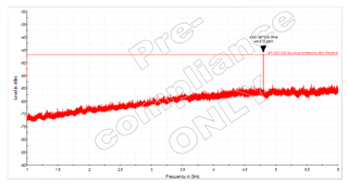
We are currently going through certification and have had an interesting failure during radiated emissions.  When in normal transceiver mode, all is well, but when we put the device into a special receiver only mode using the Wirepas tool then we fail at the second harmonic of 4.8GHz even though there are no emissions at 2.4GHz.  Very odd. 

I would have thought that, if anything, we would fail a transmitter test rather than a receiver test.  Could the emissions be coming from the receiver local oscillator?  What would you suggest to try and fix it?

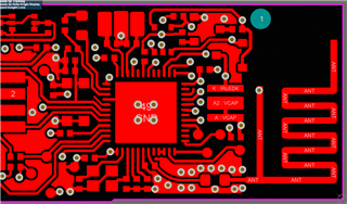
Incidentally, we are using a pretty standard meandering inverted F PCB trace antenna with parallel cap and series inductor. 

Parents
  • FormerMember
    0 FormerMember

    Yes, that emission is from the RX LO, and most likely, it's related to errata 138. The fix is to either ground P0.25 and P0.26 if the pins are not used, or place a 12 pF capacitor near the pin to ground on both pins. (See the reference layout.)

  • Hello Kristin, 

    We tested the solution today and the result was unsuccessful.  Both pins P0.25 and P0.26 are currently allocated in our design, so we put 12pf caps from these pins to ground and saw no change in the 4.8GHz emission.  We then connected these pins to ground and saw no improvement to the emission. 

    We used a near field sniffer probe for the test and it was hard to pinpoint where the source was.  We disconnected the antenna by removing the series L and that made no difference, so I presume is not coming from the antenna. 

    I have pasted an image of the top layer of our four later board for your reference. 

    This product is going into mass production in a few months time so we are really needing help to fix this issue.  Any advice you can offer is appreciated. 

    Regards

    Mike

  • Layer stack.pdf

    Hell Kristin, 

    I have uploaded the layer stack from top to bottom.  Looking forward to your advice.

  • There are significant issues with your layout. I will just go through the items I see wrong. Also, oddly you show layer one mirrored left/right.  I guess your cad app likes to think the top is the bottom and the bottom is the top?  Normally layer 1 (top) is dead on normal.  But either works as long as your board vendor is happy.

    1. Insufficient ground vias for nRF. On our own products we use a 5x5 grid of 8 mil vias for the ground slug on the nRF.  I think Nordic uses a 4x4 grid.  2x2 is just insufficient as it forces ground currents to go a long, long way to get back to the origin. This can easily cause a variety of RF noise and even RF instability.

    2. I assume that is meant to be a shorted stub tuner on your meander F-hybrid, otherwise there would be no point in the via.  But you didn't connect the via to a suitable ground.  You should double check this against your antenna design.  Maybe the via keeps the layout app happy for open stub tuners.

    3. For some reason you chose to float the flood on inner 2. For this style of layout all the inner layers should be ground.  Only if you were trying to do power planes would this not be ground, but in general power planes invite more problems than they solve.

    4. Besides your antenna probably being well tuned to 4.8GHz due to the incorrect stub tuner a big mistake is the missing ground connection at pin 32 and the 0.8pF cap that is part of the output match/harmonic filter.  Due to the poor grounding overall, it is likely the 0.8pF cap isn't doing anything at all. Thus 4.8GHz is just passing through network.

    5. And, it looks suspiciously like you intended to copy the shunt C, series L output match of the nRF52832 reference design.  But the inductor is too far away.  Changes of as little as 1mm influence the effect a reactance has in a circuit at these frequencies. So, you should double check your design with regard to the component placement.

    Hard to say what the biggest problem is for your compliance issue. Mixers really don't like a poorly matched output and in RX mode likely there are few gain stages and more coupling with what is likely a poor match at the output. This can cause the second harmonic rejection of the network to be worse.

  • FormerMember
    0 FormerMember in reply to AmbystomaLabs

    @ambystomalabs has a lot of good points.


    I would like to add: Regarding P0.25 and P0.26:

    • When adding 12 pF capacitors, they have to be added as close as possible to the pins, see the refence layout.
    • When you grounded P0.25 and P0.26, how did you do it? The very best is to ground them to the center pad.

    In addition, the routing of the RF part has to be an exact copy of our reference layout, see this tutorial, section "Matching networks"

    Regarding the antenna: the ground plane has to be extended so that the stub can be grounded.

  • Hi, 

    Thank you for taking the trouble to review the layout. Your comments have been taken on board.  The ground via on the antenna was a good pick up, it was not intended to be like that.  I will go back to the reference layout and see what improvements can be made.

  • Thank you for your additional comments, I will refer back to the reference layout.

Reply Children
No Data
Related