
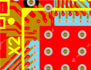
The NRF52840 appears to only come in a dual row QFN package and in the reference material, the only way to break out the second row is with an in-pad via or a very small trace. Here is an image of the pads in question for the Altium reference designs:
Via-in-pad generally require epoxy back-fill which is increases the price per PCB considerably. I was hoping to find a way to avoid pricey manufacturing processes like HDI, epoxy back-fill, blind/buried vias, etc.
One thought I had was remapping everything to the outer row. Could this be a feasibly option? In my application, I'm not using all the GPIO and can comfortably remap all my used signals to pads on the outer rows. The one signal that I'm concerned with, however, is the NRST signal on pin AC13. It looks like it can be moved with the PSELRESET[0] and PSELRESET[1] registers but I didn't know if the reset pin was needed to program a blank device (creating a chicken & egg problem).
As a side note, I was also considering wiring up the Trace port but it looks like the TRACE_CLK signal is less flexible than nRESET. I don't think that one can be moved from the inner row, but I can probably get by with other debug methods.

