Hi.
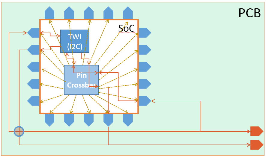
To avoid via in PAD I like to route a signal/pin from the inner row (closest to center) through a pin in the outer row. However, to be able to do that I must be sure the pins (GPIO pins) is an input after reset and when programming the device.
In my case it is for the UART and RESET pin I like to connect some pins together to be able to route them out from the package without using any via-in-PAD.
For example for the RESET pin (PAD AC13, inner row), I like to route it through the P0.17 pin (PAD AD12, outer row). This requires P0.17 is an input when programming and hence looks transparent for the RESET signal.
Schematic and layout in attached pdf. Will this approach be OK?
Best regards Joakim