This post is older than 2 years and might not be relevant anymore
More Info: Consider searching for newer posts

NRF52840 sma routing

I am designing a simple broadcaster using an sma connector for a dipole antenna.

I have added a 50 ohm SMA connector to the reference deign

.  

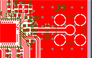
so you can see above is the placement of the SMA and the mid plane keep out. I have also added vias to join the ground planes and have omitted the bottom layer as its a complete fill.

There are vias next to the antenna feed point to join the bottom layer as much as possible.

1. Should the mid plane be bulged out for where the antenna feed pad starts to come closer?

2. is there any length considerations to the main feed line?

3. the output from the chip is from an internal balun, why are there balancing caps/conductors.

4. will this still need to be tuned for the board or is there a high likelyhood of the refrence design allready be suited for the SMA/50 ohm dipole.

Parents
  • 1. You need to have the bottom layer as solid ground plane. Technically, you don't need the cut out on the inner layers either, but it doesn't harm. The transmission line must be calculated depending on the PCB stack up. The dimensions of the transmission like hence depends if you have a cut out in the inner layers or not. 

    You want to use a "co-planar waveguide" as  the transmission line. You can find online calculators.

    2. Not unless it's very long. 

    3. The output isn't 50 ohm so some external impedance transformation is needed. The components also do low pass filtering of the harmonics. 

    4. If you follow the reference design exactly, there should be no need to tune anything.

    Using a through hole or surface mount connector matters little.

  • Thankyou for looking at this.

    I looked at the Co-planar waveguide calculations and they came up with about 60ohm.

    Calculator_1

    Calculator_2

    Relative Dielectric Constant = 4.2

    Track Width = 30mil = 0.762mm (as per reference design)

    Track Spacing = 10mil = 0.254mm (as per design rules)

    Board Height = 64mil = 1.6mm

    copper height = 1.4mil = 0.035mm

    One way I managed to get close to 50 ohms was to use 0.5mm between guide and ground plane, so this would mean using a 0.8mm board and ground plane on the 3rd layer.

    looking at the space left in the SMA connector there isn't much room to change track thickness and gaps.

    Am I simply over analysing this or will 10 ohms cause a disturbance in the signal,

    I am using rssi for distance calculation and am trying to get the most uniform and stable signal across multiple copies of this device.

Reply
  • Thankyou for looking at this.

    I looked at the Co-planar waveguide calculations and they came up with about 60ohm.

    Calculator_1

    Calculator_2

    Relative Dielectric Constant = 4.2

    Track Width = 30mil = 0.762mm (as per reference design)

    Track Spacing = 10mil = 0.254mm (as per design rules)

    Board Height = 64mil = 1.6mm

    copper height = 1.4mil = 0.035mm

    One way I managed to get close to 50 ohms was to use 0.5mm between guide and ground plane, so this would mean using a 0.8mm board and ground plane on the 3rd layer.

    looking at the space left in the SMA connector there isn't much room to change track thickness and gaps.

    Am I simply over analysing this or will 10 ohms cause a disturbance in the signal,

    I am using rssi for distance calculation and am trying to get the most uniform and stable signal across multiple copies of this device.

Children
Related