Hi,
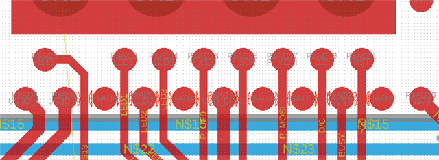
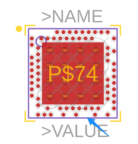
Have an issue with a prototype 2 layer 52840 pcb that i tried to get manufactured. i increased the pad diameter to 0.3mm and now i cannot route without hitting clearance limits. Is there any way around this, what should i do?
manufacturer constraints are 0.3mm pad, 3.5mil trace, 0.2mm via hole, 0.45mm via diameter.


