This post is older than 2 years and might not be relevant anymore
More Info: Consider searching for newer posts

52840 issue with pcb design

Hi,

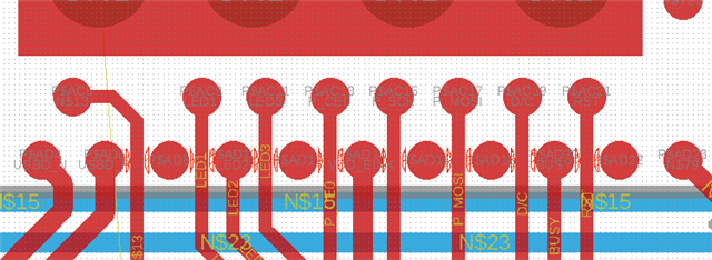
Have an issue with a prototype 2 layer 52840 pcb that i tried to get manufactured.  i increased the pad diameter to 0.3mm and now i cannot route without hitting clearance limits. Is there any way around this, what should i do?

manufacturer constraints are 0.3mm pad, 3.5mil trace, 0.2mm via hole, 0.45mm via diameter.   

Parents
  • You should review the reference design layouts. The 52840 is a fine pitch WLCSP and requires more advanced board designs. It can not be routed as you have shown.

    If you wish to do traditional drilled vias, there is only one type of design that can be done where the DCDC is not utilized and only the inner pins with a clear path and outer pins are utilized. You will find it in the reference design information in the product spec.

    To fully utilize all pins of the device, VIP (via in pad) technology must be utilized. Traditionally VIP is done with HDI (aka, laser drilled) vias. In this manner the laser drilled vias for the inner pins are directly in the center of the pad.  However, the outer pins can be routed away on the surface as normal.

    HDI(high density interconnect, aka laser drilled) is a requirement for most BGA and any WLCSP devices with multiple rows and colums of pins. Most board vendors have HDI capabilities since the technology has been around for at least 20 years now.

    HDI does require different treatments for striplines.  On HDI boards the outer layers are normally only 3 to 5 mil thickness so the laser can burn through.  As a result the ground reference is normally not on the next layer.

  • Thanks a lot! I will check the reference design and hdi.. I was thinking of removing blocking pads from footprint  as below, do you think that would work?  (or create an issue in during i.e. p&p)

Reply Children
  • Since the solder mask sits above the copper layer by ~0.8mils this means the mating ball will have to get compressed by 0.8 mils.  Likely, since the ball has no where to flow (only mask underneath and not copper) you will likely end up with shorts to neighboring pins or pins that don't connect since the die will get pushed up.

    Also the lack of symmetry in the ball arrangement may cause unexpected twisting of the part during reflow.

    I wouldn't recommend trying it.

    Either do via in pad or choose a design that doesn't require routing interior pins.

Related