This post is older than 2 years and might not be relevant anymore
More Info: Consider searching for newer posts

how to drive spi CS line low for 32 bits.

Hi,

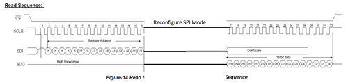
Can you please direct me to the document that explains about generating more than 8 bits of clock in SPI and keeping CS line low for that entire period.

Also, if i have to send two 16bit data, would i have to send them in lots of 8bit ? or i can send them as 16bits using nrf_drv_spi_transfer API?

I am modifying the SPI example found under SDK15/example/peripheral/spi.

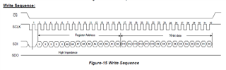
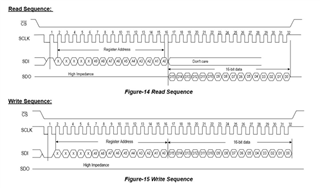
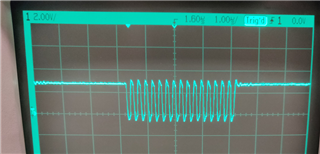
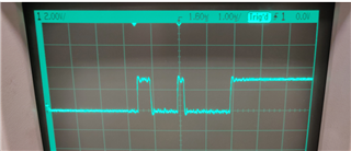
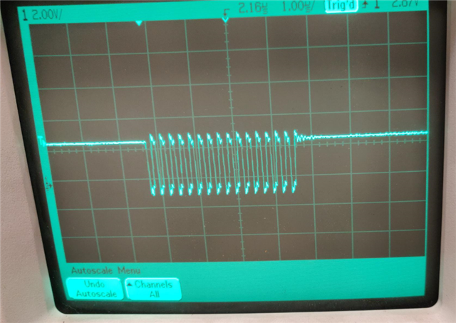
And i have to achieve the sequence attached in the image. 

Thank you  

  • Hi, I talked to the manufacturer. He asked me to check the SPI timings by doing a simple read operation on register 0x30 . I should be reading 0x6886 but i am reading 0Xffff instead. May be because of the pull up resistors on SPI pins ???

    It is a very small code base . I will be glad if you could verify for me if the code is right

    #include "nrf_drv_spi.h"
    #include "app_util_platform.h"
    #include "nrf_gpio.h"
    #include "nrf_delay.h"
    #include "boards.h"
    #include "app_error.h"
    #include <string.h>
    #include "nrf_log.h"
    #include "nrf_log_ctrl.h"
    #include "nrf_log_default_backends.h"
    
    #define SPI_INSTANCE  0 /**< SPI instance index. */
    static const nrf_drv_spi_t spi = NRF_DRV_SPI_INSTANCE(SPI_INSTANCE);  /**< SPI instance. */
    static volatile bool spi_xfer_done;  /**< Flag used to indicate that SPI instance completed the transfer. */
    
    
    static uint16_t       m_tx_buf4= 0b1000000000110000;    //0X80BC
    static uint16_t       m_tx_buf5= 0b0000000000000000;


    static uint16_t       m_rx_buf1[1];    /**< RX buffer. */
    static const uint8_t  m_length1 = 2;        /**< Transfer length. */
    
    /**
     * @brief SPI user event handler.
     * @param event
     */


    void spi_event_handler(nrf_drv_spi_evt_t const * p_event,
                           void *                    p_context)
    {
        spi_xfer_done = true;
        NRF_LOG_INFO("Transfer completed.");
        if (m_rx_buf1[0] != 0)
        {
            NRF_LOG_INFO(" Received:");
            NRF_LOG_HEXDUMP_INFO(m_rx_buf1, strlen((const char *)m_rx_buf1));
        }
    }
    
    int main(void)
    {
        bsp_board_init(BSP_INIT_LEDS);
    
        APP_ERROR_CHECK(NRF_LOG_INIT(NULL));
        NRF_LOG_DEFAULT_BACKENDS_INIT();


            nrf_drv_spi_config_t spi_config1 = NRF_DRV_SPI_DEFAULT_CONFIG;
            spi_config1.ss_pin   = NRF_DRV_SPI_PIN_NOT_USED;
            spi_config1.miso_pin = SPI_MISO_PIN;
            spi_config1.mosi_pin = SPI_MOSI_PIN;
            spi_config1.sck_pin  = SPI_SCK_PIN;
            spi_config1.mode = NRF_DRV_SPI_MODE_2;
         //   APP_ERROR_CHECK(nrf_drv_spi_init(&spi, &spi_config, spi_event_handler1, NULL));
    
            nrf_drv_spi_config_t spi_config2 = NRF_DRV_SPI_DEFAULT_CONFIG;
            spi_config2.ss_pin   = NRF_DRV_SPI_PIN_NOT_USED;
            spi_config2.miso_pin = SPI_MISO_PIN;
            spi_config2.mosi_pin = SPI_MOSI_PIN;
            spi_config2.sck_pin  = SPI_SCK_PIN;
            spi_config2.mode = NRF_DRV_SPI_MODE_3;
         //   APP_ERROR_CHECK(nrf_drv_spi_init(&spi, &spi_config, spi_event_handler1, NULL));
    
           nrf_gpio_cfg_output(29);
    
        NRF_LOG_INFO("SPI example started.");


            while(1){
    
            //initialize with spi config 1
          
            APP_ERROR_CHECK(nrf_drv_spi_init(&spi, &spi_config1, spi_event_handler, NULL));
            
    
            memset(m_rx_buf1, 0, m_length1);
            spi_xfer_done = false;
            //clear CS line
            nrf_gpio_pin_clear(29);
            //Send 80H to BCH to read power factor from BCH register
            APP_ERROR_CHECK(nrf_drv_spi_transfer(&spi, &m_tx_buf4, m_length1, m_rx_buf1, m_length1));
            NRF_LOG_FLUSH();
            bsp_board_led_invert(3);
            nrf_delay_ms(200);
    
            nrf_drv_spi_uninit(&spi);
            APP_ERROR_CHECK(nrf_drv_spi_init(&spi, &spi_config2, spi_event_handler, NULL));
              memset(m_rx_buf1, 0, m_length1);
            spi_xfer_done = false;
            APP_ERROR_CHECK(nrf_drv_spi_transfer(&spi, &m_tx_buf5, m_length1, m_rx_buf1, m_length1));
            NRF_LOG_FLUSH();
            bsp_board_led_invert(2);
            nrf_delay_ms(200);
    
            //set CS pin high again
            nrf_gpio_pin_set(29);
             
              nrf_drv_spi_uninit(&spi);


            }


    }
    
    or not .

    I am also attaching the O'scope diagrams of CLK and MOSI line .

     5277.Atmel-46004-SE-M90E36A-Datasheet.pdf

    Thanks,

  • Hi,


    Are you able to scope all SPI lines, so that we're able to see that the mode is successfully changed when reading the response from the device?

    Kind regards,

    Håkon

  • This looks like only one part of the SPI communication, the first 16 bits, where you lack the mode switch over to the last 16 bit transfer. Do you have access to a logic analyzer/oscilloscope with 4 channels, so that you can sample all lines simultaneously? 

  • Hi Hakan,

    Unfortunately I have access to only one channel oscilloscope for now. Have ordered one with 4 channels. 

    I have reduced the code base just to see the mode switch. I can only see a consistent 16bit clock with no delay as described in this attached picture. 

    The code does not work as expected . 

            nrf_drv_spi_config_t spi_config1 = NRF_DRV_SPI_DEFAULT_CONFIG;
            spi_config1.ss_pin   = NRF_DRV_SPI_PIN_NOT_USED;
            spi_config1.miso_pin = SPI_MISO_PIN;
            spi_config1.mosi_pin = SPI_MOSI_PIN;
            spi_config1.sck_pin  = SPI_SCK_PIN;
            spi_config1.mode = NRF_DRV_SPI_MODE_2;
         //   APP_ERROR_CHECK(nrf_drv_spi_init(&spi, &spi_config, spi_event_handler1, NULL));
    
            nrf_drv_spi_config_t spi_config2 = NRF_DRV_SPI_DEFAULT_CONFIG;
            spi_config2.ss_pin   = NRF_DRV_SPI_PIN_NOT_USED;
            spi_config2.miso_pin = SPI_MISO_PIN;
            spi_config2.mosi_pin = SPI_MOSI_PIN;
            spi_config2.sck_pin  = SPI_SCK_PIN;
            spi_config2.mode = NRF_DRV_SPI_MODE_3;
         //   APP_ERROR_CHECK(nrf_drv_spi_init(&spi, &spi_config, spi_event_handler1, NULL));
    
           nrf_gpio_cfg_output(29);
    
        NRF_LOG_INFO("SPI example started.");


            while(1){
    
            //initialize with spi config 1
          
            APP_ERROR_CHECK(nrf_drv_spi_init(&spi, &spi_config1, spi_event_handler, NULL));
            
    
            memset(m_rx_buf1, 0, m_length1);
            spi_xfer_done = false;
            //clear CS line
            nrf_gpio_pin_clear(29);
            //Send 80H to BCH to read power factor from BCH register
            APP_ERROR_CHECK(nrf_drv_spi_transfer(&spi, &m_tx_buf4, m_length1, m_rx_buf1, m_length1));
            NRF_LOG_FLUSH();
            bsp_board_led_invert(3);
           nrf_delay_ms(200);
    
            nrf_drv_spi_uninit(&spi);
            APP_ERROR_CHECK(nrf_drv_spi_init(&spi, &spi_config2, spi_event_handler, NULL));
              memset(m_rx_buf1, 0, m_length1);
            spi_xfer_done = false;
            APP_ERROR_CHECK(nrf_drv_spi_transfer(&spi, &m_tx_buf5, m_length1, m_rx_buf1, m_length1));
            NRF_LOG_FLUSH();
            bsp_board_led_invert(2);
            nrf_delay_ms(200);
    
            //set CS pin high again
            nrf_gpio_pin_set(29);
             
              nrf_drv_spi_uninit(&spi);


            }


    }

    Thanks,

Related