Hello All,
I have connected nRF52840 with ADXL362 over SPI, and try to read/write data on "Power Control register".
The process I follow,
1. Rest ADXL362.
2. Write data 0x02 in "Power Control register" of ADXL362.
2. Read value of "Power Control register" of ADXL362.
But every time I read data form ADXL362 I got 0x00 value.
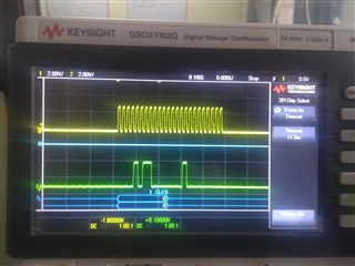
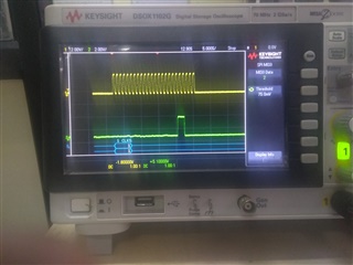
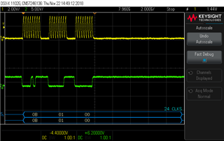
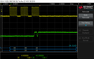
Logs are attached.
For testing this I have modify SPI test code located at "nRF5_SDK_15.0.0_a53641a\examples\peripheral\spi"
Code is also attached here, will you please guide me, If I did any wrong in SPI configuration?
I am little bit confuse of "tx_buffer_length" & "rx_buffer_length" value passing in nrf_drv_spi_transfer() function.
Does the values of "tx_buffer_length" & "rx_buffer_length" are correct at line no 101 & 118 in main.c file?
Thanks in advance.
<info> app: #########################################################
<info> app: SPI example started.
<info> SPIM: Function: nrfx_spim_init, error code: NRF_SUCCESS.
<info> app: <---- ADXL325 reset ---->
<info> SPIM: Function: spim_xfer, error code: NRF_SUCCESS.
<debug> SPIM: Event: NRF_SPIM_EVENT_END.
<info> app: Transfer completed.
<info> app:  00 00 00               |...
<info> app: soft reset
<info> app: <--- ADXL325 set power control register --->
<info> SPIM: Function: spim_xfer, error code: NRF_SUCCESS.
<info> app: ** 0 0 0
<info> app:  00 00                  |..
<info> app: Setting Measeurement Mode - Reg 2D before = 0
<debug> SPIM: Event: NRF_SPIM_EVENT_END.
<info> app: Transfer completed.
<info> app:  00 00 00               |...
<info> SPIM: Function: spim_xfer, error code: NRF_SUCCESS.
<debug> SPIM: Event: NRF_SPIM_EVENT_END.
<info> app: Transfer completed.
<info> app:  00 00 00               |...
<info> app: -----------
<info> SPIM: Function: spim_xfer, error code: NRF_SUCCESS.
<info> app: ** 0 0 0
<info> app:  00 00                  |..
<info> app: , Reg 2D after = 0
<debug> SPIM: Event: NRF_SPIM_EVENT_END.
<info> app: Transfer completed.
<info> app:  00 00 00               |...
/**
 * Copyright (c) 2015 - 2018, Nordic Semiconductor ASA
 *
 * All rights reserved.
 *
 * Redistribution and use in source and binary forms, with or without modification,
 * are permitted provided that the following conditions are met:
 *
 * 1. Redistributions of source code must retain the above copyright notice, this
 *    list of conditions and the following disclaimer.
 *
 * 2. Redistributions in binary form, except as embedded into a Nordic
 *    Semiconductor ASA integrated circuit in a product or a software update for
 *    such product, must reproduce the above copyright notice, this list of
 *    conditions and the following disclaimer in the documentation and/or other
 *    materials provided with the distribution.
 *
 * 3. Neither the name of Nordic Semiconductor ASA nor the names of its
 *    contributors may be used to endorse or promote products derived from this
 *    software without specific prior written permission.
 *
 * 4. This software, with or without modification, must only be used with a
 *    Nordic Semiconductor ASA integrated circuit.
 *
 * 5. Any software provided in binary form under this license must not be reverse
 *    engineered, decompiled, modified and/or disassembled.
 *
 * THIS SOFTWARE IS PROVIDED BY NORDIC SEMICONDUCTOR ASA "AS IS" AND ANY EXPRESS
 * OR IMPLIED WARRANTIES, INCLUDING, BUT NOT LIMITED TO, THE IMPLIED WARRANTIES
 * OF MERCHANTABILITY, NONINFRINGEMENT, AND FITNESS FOR A PARTICULAR PURPOSE ARE
 * DISCLAIMED. IN NO EVENT SHALL NORDIC SEMICONDUCTOR ASA OR CONTRIBUTORS BE
 * LIABLE FOR ANY DIRECT, INDIRECT, INCIDENTAL, SPECIAL, EXEMPLARY, OR
 * CONSEQUENTIAL DAMAGES (INCLUDING, BUT NOT LIMITED TO, PROCUREMENT OF SUBSTITUTE
 * GOODS OR SERVICES; LOSS OF USE, DATA, OR PROFITS; OR BUSINESS INTERRUPTION)
 * HOWEVER CAUSED AND ON ANY THEORY OF LIABILITY, WHETHER IN CONTRACT, STRICT
 * LIABILITY, OR TORT (INCLUDING NEGLIGENCE OR OTHERWISE) ARISING IN ANY WAY OUT
 * OF THE USE OF THIS SOFTWARE, EVEN IF ADVISED OF THE POSSIBILITY OF SUCH DAMAGE.
 *
 */
#include "nrf_drv_spi.h"
#include "app_util_platform.h"
#include "nrf_gpio.h"
#include "nrf_delay.h"
#include "boards.h"
#include "app_error.h"
#include <string.h>
#include "nrf_log.h"
#include "nrf_log_ctrl.h"
#include "nrf_log_default_backends.h"

#define SPI_INSTANCE  0 /**< SPI instance index. */
static const nrf_drv_spi_t spi = NRF_DRV_SPI_INSTANCE(SPI_INSTANCE);  /**< SPI instance. */
static volatile bool spi_xfer_done;  /**< Flag used to indicate that SPI instance completed the transfer. */

#define TEST_STRING "Nordic"
static uint8_t       m_tx_buf[] = TEST_STRING;           /**< TX buffer. */
static uint8_t       m_rx_buf[sizeof(TEST_STRING) + 1];    /**< RX buffer. */
static const uint8_t m_length = sizeof(m_tx_buf);        /**< Transfer length. */

uint8_t tx[3] = { 0x0B, 0x00, 0x00 };
uint8_t rx[3] = { 0 };


/**
 * @brief SPI user event handler.
 * @param event
 */
void spi_event_handler(nrf_drv_spi_evt_t const * p_event,
                       void *                    p_context)
{
    spi_xfer_done = true;
    NRF_LOG_INFO("Transfer completed.");
    //NRF_LOG_INFO("%d.", p_event->type);
    //NRF_LOG_INFO("%d %d %s", p_event->data.done.rx_length, p_event->data.done.tx_length, p_event->data.done.p_tx_buffer);
//    if (m_rx_buf[0] != 0)
    if (rx[0] != 0)
    {
        NRF_LOG_INFO(" Received:");
        NRF_LOG_HEXDUMP_INFO(m_rx_buf, strlen((const char *)m_rx_buf));
    }
   NRF_LOG_HEXDUMP_INFO(rx, 3);
}


#define XL362_REG_WRITE          0x0a
#define XL362_REG_READ           0x0b
#define XL362_POWER_CTL          0x2d
#define XL362_SOFT_RESET         0x1f
#define XL362_SOFT_RESET_KEY     0x52

uint8_t adxl362_read_one_reg(uint8_t reg_address)
{
  uint8_t tx_buff[3] = {0};
  uint8_t rx_buff[3] = {0};

  // </CS down> <command byte (0x0A or 0x0B)> <address byte> <data byte> <additional data bytes for multi-byte> � </CS up>
  tx_buff[0] = XL362_REG_READ;
  tx_buff[1] = reg_address;
  tx_buff[2] = 0x00;            // dummy byte

   APP_ERROR_CHECK(nrf_drv_spi_transfer(&spi, tx_buff, 3, rx_buff, 1));
   NRF_LOG_INFO("** %d %d %d", rx[0], rx[1], rx[2]);
   NRF_LOG_HEXDUMP_INFO(rx, 2);

   return rx_buff[2];
}

void adxl362_write_one_reg(uint8_t reg_address, uint8_t reg_value)
{
  uint8_t tx_buff[3] = {0};
  uint8_t rx_buff[3] = {0};

  // </CS down> <command byte (0x0A or 0x0B)> <address byte> <data byte> <additional data bytes for multi-byte> � </CS up>
  tx_buff[0] = XL362_REG_WRITE;
  tx_buff[1] = reg_address;
  tx_buff[2] = reg_value;

   APP_ERROR_CHECK(nrf_drv_spi_transfer(&spi, tx_buff, 3, rx_buff, 3));
//   NRF_LOG_INFO("** %d %d %d", rx[0], rx[1], rx[2]);
//   NRF_LOG_HEXDUMP_INFO(rx, 2);
}

void adxl362_reset()
{
  // soft reset
  adxl362_write_one_reg(XL362_SOFT_RESET, XL362_SOFT_RESET_KEY);

  // Note: A latency of approximately 0.5 ms is required after soft reset.
  nrf_delay_ms(200);
  NRF_LOG_INFO("soft reset");
}

void beginMeasure()
{
  uint8_t reg_val = 0x0;
  // read Reg 2D before modifying for measure mode
  reg_val = adxl362_read_one_reg(XL362_POWER_CTL);

  NRF_LOG_INFO("Setting Measeurement Mode - Reg 2D before = %d", reg_val);

  // turn on measurement mode
  uint8_t temp_write = (reg_val | 0x02);  // turn on measurement bit in Reg 2D

  adxl362_write_one_reg(XL362_POWER_CTL, temp_write);

  nrf_delay_ms(10);
  //nrf_delay_ms(200);

  NRF_LOG_INFO("-----------");
  // read Reg 2D before modifying for measure mode
  reg_val = adxl362_read_one_reg(XL362_POWER_CTL);
  NRF_LOG_INFO(", Reg 2D after = %d", reg_val);
}

int main(void)
{
    bsp_board_init(BSP_INIT_LEDS);

    APP_ERROR_CHECK(NRF_LOG_INIT(NULL));
    NRF_LOG_DEFAULT_BACKENDS_INIT();

    NRF_LOG_INFO("#########################################################");
    NRF_LOG_INFO("SPI example started.");

    nrf_drv_spi_config_t spi_config = NRF_DRV_SPI_DEFAULT_CONFIG;
#if 1
    spi_config.ss_pin   = NRF_GPIO_PIN_MAP(0,17);       //17
    spi_config.miso_pin = NRF_GPIO_PIN_MAP(0,23);       //23
    spi_config.mosi_pin = NRF_GPIO_PIN_MAP(0,21);       //21
    spi_config.sck_pin  = NRF_GPIO_PIN_MAP(0,19);       //19
#else
    spi_config.ss_pin   = SPI_SS_PIN;
    spi_config.miso_pin = SPI_MOSI_PIN;
    spi_config.mosi_pin = SPI_MISO_PIN;
    spi_config.sck_pin  = SPI_SCK_PIN;
#endif

    spi_config.frequency = NRF_SPIM_FREQ_1M;
//    spi_config.bit_order    = NRF_DRV_SPI_BIT_ORDER_LSB_FIRST;
//    spi_config.irq_priority = NRFX_SPIM_DEFAULT_CONFIG_IRQ_PRIORITY;
//    spi_config.mode = NRF_SPIM_MODE_3;

     ret_code_t ret = nrf_drv_spi_init(&spi, &spi_config, spi_event_handler, NULL);
     if(ret != NRF_SUCCESS)
        NRF_LOG_INFO("SPI init failed:  %d", ret);
    //APP_ERROR_CHECK(nrf_drv_spi_init(&spi, &spi_config, NULL, NULL));

    NRF_LOG_INFO("<---- ADXL325 reset ---->");
    adxl362_reset();

    NRF_LOG_INFO("<--- ADXL325 set power control register --->");
    beginMeasure();

    while (1)
    {
#if 0
        // Reset rx buffer and transfer done flag
        memset(m_rx_buf, 0, m_length);
        spi_xfer_done = false;

//        APP_ERROR_CHECK(nrf_drv_spi_transfer(&spi, tx, 3, rx, 3));
          nrf_drv_spi_transfer(&spi, tx, 3, rx, 1);

        NRF_LOG_INFO("SPI tx: %d", ret);

        NRF_LOG_INFO("** %d %d %d", rx[0], rx[1], rx[2]);
//        NRF_LOG_HEXDUMP_INFO(rx, 2);

        // read Reg 2D before modifying for measure mode
      uint8_t  reg_val = adxl362_read_one_reg(XL362_POWER_CTL);
      NRF_LOG_INFO(", Reg 2D after = %d", reg_val);
#endif
        while (!spi_xfer_done)
        {
            __WFE();
        }

        NRF_LOG_FLUSH();

//        bsp_board_led_invert(BSP_BOARD_LED_0);
        nrf_delay_ms(200);
    }
}