Hello sir,
I am a beginner on NRF52840. I am using Nrfx_spim example for interfacing sensor with NRF Board.
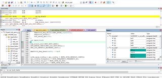
I have done some driver about Reg_read and Reg_write. I tried to read the device ID of the sensor through SPI yielding improper results.
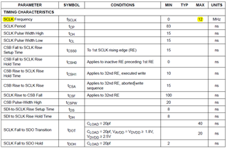
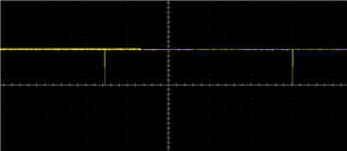
Hence I probed on the SPI_SCK line and I found that the duty cycle of SPI_SCK is not proper and also set up and hold times are not proper.
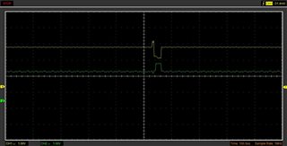
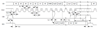
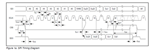
In my requirement timing of the SPI should be as in the attached image below.

To be more specific I need to meet the timing requirements as of detailed in the image below.
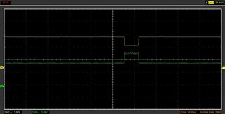
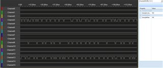
Presently The waveform what I am observing on probing SPI_SCK is as below.
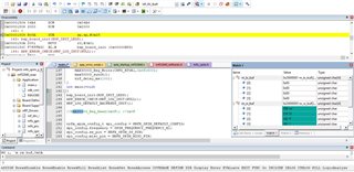
I am pretty sure that my SPI configurations are not proper, please provide me a pointer where I can do the SPI configurations to meet the timing requirements detailed above.
Expecting your kind help.
Thanks,
Rohit