This post is older than 2 years and might not be relevant anymore
More Info: Consider searching for newer posts

How to change qspi_pca10056 pin setting and command setting

Hi Guys,

I'm interested to get guideline on how could I customized the qspi example from nordic in terms of pins and command. I don't see any different between MX25R6435F vs S25FL064L chipset

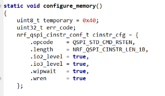
I was trying to change the qspi example code and unsuccessful control the qspi using the following setting.

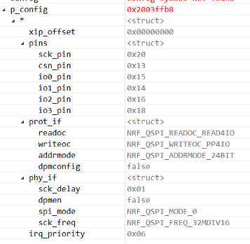
#define QSPI_CSN NRF_GPIO_PIN_MAP(0,19)
#define QSPI_IO0 NRF_GPIO_PIN_MAP(0,21)
#define QSPI_IO1 NRF_GPIO_PIN_MAP(0,20)
#define QSPI_IO2 NRF_GPIO_PIN_MAP(0,22)
#define QSPI_IO3 NRF_GPIO_PIN_MAP(0,24)
#define QSPI_SCK NRF_GPIO_PIN_MAP(1,0)

And the I did some change to some of the header as below

nrfx_qspi.h

#define NRFX_QSPI_DEFAULT_CONFIG                                        \
{                                                                       \
    .xip_offset  = NRFX_QSPI_CONFIG_XIP_OFFSET,                         \
    .pins = {                                                           \
       .sck_pin     = QSPI_PIN_SCK,                                \
       .csn_pin     = QSPI_PIN_CSN,                                \
       .io0_pin     = QSPI_PIN_IO0,                                \
       .io1_pin     = QSPI_PIN_IO1,                                \
       .io2_pin     = QSPI_PIN_IO2,                                \
       .io3_pin     = QSPI_PIN_IO3,                                \
    },                                                                  \
    .irq_priority   = (uint8_t)NRFX_QSPI_CONFIG_IRQ_PRIORITY,           \
    .prot_if = {                                                        \
        .readoc     = (nrf_qspi_readoc_t)NRFX_QSPI_CONFIG_READOC,       \
        .writeoc    = (nrf_qspi_writeoc_t)NRFX_QSPI_CONFIG_WRITEOC,     \
        .addrmode   = (nrf_qspi_addrmode_t)NRFX_QSPI_CONFIG_ADDRMODE,   \
        .dpmconfig  = false,                                            \
    },                                                                  \
    .phy_if = {                                                         \
        .sck_freq   = (nrf_qspi_frequency_t)NRFX_QSPI_CONFIG_FREQUENCY, \
        .sck_delay  = (uint8_t)NRFX_QSPI_CONFIG_SCK_DELAY,              \
        .spi_mode   = (nrf_qspi_spi_mode_t)NRFX_QSPI_CONFIG_MODE,       \
        .dpmen      = false                                             \
    },                                                                  \
}

nrf_drv_qspi.h

#if QSPI_PIN_SCK == NRF_QSPI_PIN_NOT_CONNECTED
    #undef QSPI_PIN_SCK
    #define QSPI_PIN_SCK  QSPI_PIN_SCK
#endif
#if QSPI_PIN_CSN == NRF_QSPI_PIN_NOT_CONNECTED
    #undef QSPI_PIN_CSN
    #define QSPI_PIN_CSN  QSPI_PIN_CSN
#endif
#if QSPI_PIN_IO0 == NRF_QSPI_PIN_NOT_CONNECTED
    #undef QSPI_PIN_IO0
    #define QSPI_PIN_IO0  QSPI_PIN_IO0
#endif
#if QSPI_PIN_IO1 == NRF_QSPI_PIN_NOT_CONNECTED
    #undef QSPI_PIN_IO1
    #define QSPI_PIN_IO1  QSPI_PIN_IO1
#endif
#if QSPI_PIN_IO2 == NRF_QSPI_PIN_NOT_CONNECTED
    #undef QSPI_PIN_IO2
    #define QSPI_PIN_IO2  QSPI_PIN_IO2
#endif
#if QSPI_PIN_IO3 == NRF_QSPI_PIN_NOT_CONNECTED
    #undef QSPI_PIN_IO3
    #define QSPI_PIN_IO3  QSPI_PIN_IO3
#endif

Target memory chip to use.

http://www.cypress.com/file/316661/download

Parents
  • Hi Guys,

    After I read some info from the following page.

    https://community.nxp.com/thread/336422

    I modify the qspi_bootloader_pca10056 example code to reprogram the chip into quad-spi mode. The result still no data capture on SO1 pin when I trigger nrf_drv_qspi_write.

    The modify I did to qspi_bootloader_pca10056 is as below. I changed the BSP_QSPI_ pin to support the new memory chip.

    ..\components\boards\pca10056.h

    /**
     * Copyright (c) 2016 - 2018, Nordic Semiconductor ASA
     *
     * All rights reserved.
     *
     * Redistribution and use in source and binary forms, with or without modification,
     * are permitted provided that the following conditions are met:
     *
     * 1. Redistributions of source code must retain the above copyright notice, this
     *    list of conditions and the following disclaimer.
     *
     * 2. Redistributions in binary form, except as embedded into a Nordic
     *    Semiconductor ASA integrated circuit in a product or a software update for
     *    such product, must reproduce the above copyright notice, this list of
     *    conditions and the following disclaimer in the documentation and/or other
     *    materials provided with the distribution.
     *
     * 3. Neither the name of Nordic Semiconductor ASA nor the names of its
     *    contributors may be used to endorse or promote products derived from this
     *    software without specific prior written permission.
     *
     * 4. This software, with or without modification, must only be used with a
     *    Nordic Semiconductor ASA integrated circuit.
     *
     * 5. Any software provided in binary form under this license must not be reverse
     *    engineered, decompiled, modified and/or disassembled.
     *
     * THIS SOFTWARE IS PROVIDED BY NORDIC SEMICONDUCTOR ASA "AS IS" AND ANY EXPRESS
     * OR IMPLIED WARRANTIES, INCLUDING, BUT NOT LIMITED TO, THE IMPLIED WARRANTIES
     * OF MERCHANTABILITY, NONINFRINGEMENT, AND FITNESS FOR A PARTICULAR PURPOSE ARE
     * DISCLAIMED. IN NO EVENT SHALL NORDIC SEMICONDUCTOR ASA OR CONTRIBUTORS BE
     * LIABLE FOR ANY DIRECT, INDIRECT, INCIDENTAL, SPECIAL, EXEMPLARY, OR
     * CONSEQUENTIAL DAMAGES (INCLUDING, BUT NOT LIMITED TO, PROCUREMENT OF SUBSTITUTE
     * GOODS OR SERVICES; LOSS OF USE, DATA, OR PROFITS; OR BUSINESS INTERRUPTION)
     * HOWEVER CAUSED AND ON ANY THEORY OF LIABILITY, WHETHER IN CONTRACT, STRICT
     * LIABILITY, OR TORT (INCLUDING NEGLIGENCE OR OTHERWISE) ARISING IN ANY WAY OUT
     * OF THE USE OF THIS SOFTWARE, EVEN IF ADVISED OF THE POSSIBILITY OF SUCH DAMAGE.
     *
     */
    #ifndef PCA10056_H
    #define PCA10056_H
    
    #ifdef __cplusplus
    extern "C" {
    #endif
    
    #include "nrf_gpio.h"
    
    // LEDs definitions for PCA10056
    #define LEDS_NUMBER    4
    
    #define LED_1          NRF_GPIO_PIN_MAP(0,13)
    #define LED_2          NRF_GPIO_PIN_MAP(0,14)
    #define LED_3          NRF_GPIO_PIN_MAP(0,15)
    #define LED_4          NRF_GPIO_PIN_MAP(0,16)
    
    #define LED_START      LED_1
    #define LED_STOP       LED_4
    
    #define LEDS_ACTIVE_STATE 0
    
    //#define LEDS_LIST { LED_1, LED_2, LED_3, LED_4 }
    #define LEDS_LIST { LED_1, LED_2, LED_3}
    
    #define LEDS_INV_MASK  LEDS_MASK
    
    #define BSP_LED_0      13
    #define BSP_LED_1      14
    #define BSP_LED_2      15
    #define BSP_LED_3      16
    
    #define BUTTONS_NUMBER 4
    
    #define BUTTON_1       11
    #define BUTTON_2       12
    #define BUTTON_3       24
    #define BUTTON_4       25
    #define BUTTON_PULL    NRF_GPIO_PIN_PULLUP
    
    #define BUTTONS_ACTIVE_STATE 0
    
    #define BUTTONS_LIST { BUTTON_1, BUTTON_2, BUTTON_3, BUTTON_4 }
    
    #define BSP_BUTTON_0   BUTTON_1
    #define BSP_BUTTON_1   BUTTON_2
    #define BSP_BUTTON_2   BUTTON_3
    #define BSP_BUTTON_3   BUTTON_4
    
    #define RX_PIN_NUMBER  8
    #define TX_PIN_NUMBER  6
    #define CTS_PIN_NUMBER 7
    #define RTS_PIN_NUMBER 5
    #define HWFC           true
    
    //#define BSP_QSPI_SCK_PIN   19
    //#define BSP_QSPI_CSN_PIN   17
    //#define BSP_QSPI_IO0_PIN   20
    //#define BSP_QSPI_IO1_PIN   21
    //#define BSP_QSPI_IO2_PIN   22
    //#define BSP_QSPI_IO3_PIN   23
    
    #define BSP_QSPI_SCK_PIN   NRF_GPIO_PIN_MAP(1,12)
    #define BSP_QSPI_CSN_PIN   NRF_GPIO_PIN_MAP(0,19)
    #define BSP_QSPI_IO0_PIN   NRF_GPIO_PIN_MAP(0,21)
    #define BSP_QSPI_IO1_PIN   NRF_GPIO_PIN_MAP(0,20)
    #define BSP_QSPI_IO2_PIN   NRF_GPIO_PIN_MAP(0,22)
    #define BSP_QSPI_IO3_PIN   NRF_GPIO_PIN_MAP(0,25)
    
    // serialization APPLICATION board - temp. setup for running serialized MEMU tests
    #define SER_APP_RX_PIN              NRF_GPIO_PIN_MAP(1,13)    // UART RX pin number.
    #define SER_APP_TX_PIN              NRF_GPIO_PIN_MAP(1,14)    // UART TX pin number.
    #define SER_APP_CTS_PIN             NRF_GPIO_PIN_MAP(0,2)     // UART Clear To Send pin number.
    #define SER_APP_RTS_PIN             NRF_GPIO_PIN_MAP(1,15)    // UART Request To Send pin number.
    
    #define SER_APP_SPIM0_SCK_PIN       NRF_GPIO_PIN_MAP(0,27)     // SPI clock GPIO pin number.
    #define SER_APP_SPIM0_MOSI_PIN      NRF_GPIO_PIN_MAP(0,2)      // SPI Master Out Slave In GPIO pin number
    #define SER_APP_SPIM0_MISO_PIN      NRF_GPIO_PIN_MAP(0,26)     // SPI Master In Slave Out GPIO pin number
    #define SER_APP_SPIM0_SS_PIN        NRF_GPIO_PIN_MAP(1,13)     // SPI Slave Select GPIO pin number
    #define SER_APP_SPIM0_RDY_PIN       NRF_GPIO_PIN_MAP(1,15)     // SPI READY GPIO pin number
    #define SER_APP_SPIM0_REQ_PIN       NRF_GPIO_PIN_MAP(1,14)     // SPI REQUEST GPIO pin number
    
    // serialization CONNECTIVITY board
    #define SER_CON_RX_PIN              NRF_GPIO_PIN_MAP(1,14)    // UART RX pin number.
    #define SER_CON_TX_PIN              NRF_GPIO_PIN_MAP(1,13)    // UART TX pin number.
    #define SER_CON_CTS_PIN             NRF_GPIO_PIN_MAP(1,15)    // UART Clear To Send pin number. Not used if HWFC is set to false.
    #define SER_CON_RTS_PIN             NRF_GPIO_PIN_MAP(0,2)     // UART Request To Send pin number. Not used if HWFC is set to false.
    
    
    #define SER_CON_SPIS_SCK_PIN        NRF_GPIO_PIN_MAP(0,27)    // SPI SCK signal.
    #define SER_CON_SPIS_MOSI_PIN       NRF_GPIO_PIN_MAP(0,2)     // SPI MOSI signal.
    #define SER_CON_SPIS_MISO_PIN       NRF_GPIO_PIN_MAP(0,26)    // SPI MISO signal.
    #define SER_CON_SPIS_CSN_PIN        NRF_GPIO_PIN_MAP(1,13)    // SPI CSN signal.
    #define SER_CON_SPIS_RDY_PIN        NRF_GPIO_PIN_MAP(1,15)    // SPI READY GPIO pin number.
    #define SER_CON_SPIS_REQ_PIN        NRF_GPIO_PIN_MAP(1,14)    // SPI REQUEST GPIO pin number.
    
    #define SER_CONN_CHIP_RESET_PIN     NRF_GPIO_PIN_MAP(1,1)    // Pin used to reset connectivity chip
    
    // Arduino board mappings
    #define ARDUINO_SCL_PIN             27    // SCL signal pin
    #define ARDUINO_SDA_PIN             26    // SDA signal pin
    #define ARDUINO_AREF_PIN            2     // Aref pin
    
    #define ARDUINO_13_PIN              NRF_GPIO_PIN_MAP(1, 15)  // Digital pin 13
    #define ARDUINO_12_PIN              NRF_GPIO_PIN_MAP(1, 14)  // Digital pin 12
    #define ARDUINO_11_PIN              NRF_GPIO_PIN_MAP(1, 13)  // Digital pin 11
    #define ARDUINO_10_PIN              NRF_GPIO_PIN_MAP(1, 12)  // Digital pin 10
    #define ARDUINO_9_PIN               NRF_GPIO_PIN_MAP(1, 11)  // Digital pin 9
    #define ARDUINO_8_PIN               NRF_GPIO_PIN_MAP(1, 10)  // Digital pin 8
    
    #define ARDUINO_7_PIN               NRF_GPIO_PIN_MAP(1, 8) // Digital pin 7
    #define ARDUINO_6_PIN               NRF_GPIO_PIN_MAP(1, 7) // Digital pin 6
    #define ARDUINO_5_PIN               NRF_GPIO_PIN_MAP(1, 6) // Digital pin 5
    #define ARDUINO_4_PIN               NRF_GPIO_PIN_MAP(1, 5) // Digital pin 4
    #define ARDUINO_3_PIN               NRF_GPIO_PIN_MAP(1, 4) // Digital pin 3
    #define ARDUINO_2_PIN               NRF_GPIO_PIN_MAP(1, 3) // Digital pin 2
    #define ARDUINO_1_PIN               NRF_GPIO_PIN_MAP(1, 2) // Digital pin 1
    #define ARDUINO_0_PIN               NRF_GPIO_PIN_MAP(1, 1) // Digital pin 0
    
    #define ARDUINO_A0_PIN              3     // Analog channel 0
    #define ARDUINO_A1_PIN              4     // Analog channel 1
    #define ARDUINO_A2_PIN              28    // Analog channel 2
    #define ARDUINO_A3_PIN              29    // Analog channel 3
    #define ARDUINO_A4_PIN              30    // Analog channel 4
    #define ARDUINO_A5_PIN              31    // Analog channel 5
    
    //MWDS device mappings
    #define PMIC_INT        NRF_GPIO_PIN_MAP(0,29)
    #define PMIC_NRESET     NRF_GPIO_PIN_MAP(0,12)
    #define PMIC_NPG        NRF_GPIO_PIN_MAP(1,15)
    #define PMIC_NCD        NRF_GPIO_PIN_MAP(1,13)
    #define ACC_INT         NRF_GPIO_PIN_MAP(0,26)
    /* PMIC and Accelerometer I2c port1*/
    #define I2C_PORT2_SCL_PIN             NRF_GPIO_PIN_MAP(0,15)    // SCL signal pin
    #define I2C_PORT2_SDA_PIN             NRF_GPIO_PIN_MAP(0,13)    // SDA signal pin
    
    #define LED_RED         NRF_GPIO_PIN_MAP(0,6)
    #define LED_BLU         NRF_GPIO_PIN_MAP(0,8)
    #define LED_GRN         NRF_GPIO_PIN_MAP(1,9)
    #define NCHG            NRF_GPIO_PIN_MAP(0,11)
    /* PMIC and Accelerometer I2c port1*/
    #define I2C_PORT1_SCL_PIN             NRF_GPIO_PIN_MAP(0,5)    // SCL signal pin
    #define I2C_PORT1_SDA_PIN             NRF_GPIO_PIN_MAP(0,27)    // SDA signal pin
    #define NRF_NRESET      NRF_GPIO_PIN_MAP(0,18)
    #define MWDS_QSPI_NCS        NRF_GPIO_PIN_MAP(0,19)
    #define MWDS_QSPI_IO0        NRF_GPIO_PIN_MAP(0,21)
    #define MWDS_QSPI_IO1        NRF_GPIO_PIN_MAP(0,20)
    #define MWDS_QSPI_IO2        NRF_GPIO_PIN_MAP(0,22)
    #define MWDS_QSPI_IO3        NRF_GPIO_PIN_MAP(0,24)
    #define MWDS_QSPI_SCK        NRF_GPIO_PIN_MAP(1,0)
    #define NMR             NRF_GPIO_PIN_MAP(1,2)
    
    #ifdef __cplusplus
    }
    #endif
    
    #endif // PCA10056_H
    

    Please advice me.

    Thanks.

  • Hi,

    Are you using an nRF52840 DK? Have you studied the Connector interface and checked whether the pins you are using are not already used for something else? Note also that the pins used for the memory chip on the DK is not routed to the connectors along the edge. If you want the pins connected to the connectors you will have to cut and solder some solder bridges

  • Hi 

    Thanks for the quick reply. Our hardware team already free up those port and connect it to the new memory chip. The modification is based on PCA10056_schematic_and_pcb.pdf from nordic website.

    And we did managed to recapture write output on the pin on SI0,SI1,SI2,SI3,CLK and CS

    I suspect there are some address different in pre configure the chip to enter quad mode spi

    Here is some link info about the chip I using now.

    https://community.cypress.com/docs/DOC-15299

    May I know how can I decode the info for .io2_level,io3_level,wipwait,wren. Where can I change the address? And what is the temporary = 0x40 use for?

    what is NRF_QSPI_BASE? Was it part of the QSPI address in the nrf52840 transmit buffer? I notice those nrf_qsi_cinstr_conf_t value were convert into binary and store in the NRF_QSPI_BASE.

  • what is NRF_QSPI_BASE? 
    It is the base address of the QSPI peripheral in HW:
    nrf52840.h:

    #define NRF_QSPI_BASE               0x40029000UL

    And what is the temporary = 0x40 use for?
    It is the value written to the Status Register in the memory chip on the nRF52840 DK to enable quad SPI (the writer of the example could have chosen a better variable name). From the MX25R6435F datasheet:

    May I know how can I decode the info for .io2_level,io3_level,wipwait,wren.
    What do you mean by decode? If you wonder what the fields are for then maybe the documentation can help. 

    I suspect there are some address different in pre configure the chip to enter quad mode spi
    There seems to be some differences between the two memory chips, but it also seems pretty clearly documented in your link:

    1. Initiate the WREN (05h) ....
    2. Initiate the WRR (01h) command; input “02h” (for SR1NV[1]); input “02h” (for CR1NV[1]); input “68h” (for CR2NV[3]) .....
  • Hi 

    Thanks for the the info. I tried the following step before, it just didn't workout well where the data always inconsistent.

    1. Initiate the WREN (05h) ....
    2. Initiate the WRR (01h) command; input “02h” (for SR1NV[1]); input “02h” (for CR1NV[1]); input “68h” (for CR2NV[3]) .....

    #define QSPI_STD_CMD_WRR   0x01
    #define QSPI_STD_CMD_RSTEN  0x66
    #define QSPI_STD_CMD_RST    0x99
    
    static void configure_memory()
    
    {
    
        uint8_t temporary[4] = {0x02,0x02,0x68,0x78};
    
        uint32_t err_code;
    
        nrf_qspi_cinstr_conf_t cinstr_cfg = {
    
            .opcode    = QSPI_STD_CMD_RSTEN,
    
            .length    = NRF_QSPI_CINSTR_LEN_1B,
    
            .io2_level = true,
    
            .io3_level = true,
    
            .wipwait   = true,
    
            .wren      = true
    
        };


        // Send reset enable
    
        err_code = nrf_drv_qspi_cinstr_xfer(&cinstr_cfg, NULL, NULL);
    
        APP_ERROR_CHECK(err_code);


        // Send reset command
    
        cinstr_cfg.opcode = QSPI_STD_CMD_RST;
    
        err_code = nrf_drv_qspi_cinstr_xfer(&cinstr_cfg, NULL, NULL);
    
        APP_ERROR_CHECK(err_code);


        // Send WREN
    
        cinstr_cfg.opcode = 0x06;
    
        err_code = nrf_drv_qspi_cinstr_xfer(&cinstr_cfg, NULL, NULL);
    
        APP_ERROR_CHECK(err_code);


        // Switch to qspi mode
    
        cinstr_cfg.opcode = QSPI_STD_CMD_WRR;
    
        cinstr_cfg.length = NRF_QSPI_CINSTR_LEN_5B;
    
        err_code = nrf_drv_qspi_cinstr_xfer(&cinstr_cfg, &temporary, NULL);
    
        APP_ERROR_CHECK(err_code);
    
    }


    int main(void)
    
    {
    
        uint32_t i;
    
        ret_code_t err_code;
    
        srand(0);
    
        for (i = 0; i < QSPI_TEST_DATA_SIZE; ++i)
    
        {
    
            m_buffer_tx[i] = (uint8_t)rand();
    
        }


          nrf_drv_qspi_config_t config = NRF_DRV_QSPI_DEFAULT_CONFIG;
    
        err_code = nrf_drv_qspi_init(&config, qspi_handler, NULL);
    
        APP_ERROR_CHECK(err_code);
    
        NRF_LOG_INFO("QSPI example started.");


        configure_memory();


        m_finished = false;
    
        err_code = nrf_drv_qspi_erase(NRF_QSPI_ERASE_LEN_64KB, 0);
    
        APP_ERROR_CHECK(err_code);
    
        WAIT_FOR_PERIPH();
    
        NRF_LOG_INFO("Process of erasing first block start");


        err_code = nrf_drv_qspi_write(m_buffer_tx, QSPI_TEST_DATA_SIZE, 0);
    
        APP_ERROR_CHECK(err_code);
    
        WAIT_FOR_PERIPH();
    
        NRF_LOG_INFO("Process of writing data start");


        err_code = nrf_drv_qspi_read(m_buffer_rx, QSPI_TEST_DATA_SIZE, 0);
    
        WAIT_FOR_PERIPH();
    
        NRF_LOG_INFO("Data read");


        NRF_LOG_INFO("Compare...");
    
        if (memcmp(m_buffer_tx, m_buffer_rx, QSPI_TEST_DATA_SIZE) == 0)
    
        {
    
            NRF_LOG_INFO("Data consistent");
    
        }
    
        else
    
        {
    
            NRF_LOG_INFO("Data inconsistent");
    
        }


    }


    I have another 2 question about the following code.

    Under nrfx_qspi.h, do we need to modify the value for READOC and WRITEOC?

    #define NRFX_QSPI_DEFAULT_CONFIG                                        \
    {                                                                       \
        .xip_offset  = NRFX_QSPI_CONFIG_XIP_OFFSET,                         \
        .pins = {                                                           \
           .sck_pin     = NRFX_QSPI_PIN_SCK,                                \
           .csn_pin     = NRFX_QSPI_PIN_CSN,                                \
           .io0_pin     = NRFX_QSPI_PIN_IO0,                                \
           .io1_pin     = NRFX_QSPI_PIN_IO1,                                \
           .io2_pin     = NRFX_QSPI_PIN_IO2,                                \
           .io3_pin     = NRFX_QSPI_PIN_IO3,                                \
        },                                                                  \
        .irq_priority   = (uint8_t)NRFX_QSPI_CONFIG_IRQ_PRIORITY,           \
        .prot_if = {                                                        \
            .readoc     = (nrf_qspi_readoc_t)NRFX_QSPI_CONFIG_READOC,       \
            .writeoc    = (nrf_qspi_writeoc_t)NRFX_QSPI_CONFIG_WRITEOC,     \
            .addrmode   = (nrf_qspi_addrmode_t)NRFX_QSPI_CONFIG_ADDRMODE,   \
            .dpmconfig  = false,                                            \
        },                                                                  \
        .phy_if = {                                                         \
            .sck_freq   = (nrf_qspi_frequency_t)NRFX_QSPI_CONFIG_FREQUENCY, \
            .sck_delay  = (uint8_t)NRFX_QSPI_CONFIG_SCK_DELAY,              \
            .spi_mode   = (nrf_qspi_spi_mode_t)NRFX_QSPI_CONFIG_MODE,       \
            .dpmen      = false                                             \
        },                                                                  \
    }
    

    Under nrf52840_bitfields.h there are WREN and WIPWAIT which the nordic help page didn't not disclose much, do I need to modify those value based on the following table

    /* Bit 15 : Send WREN (write enable opcode 0x06) before instruction. */
    #define QSPI_CINSTRCONF_WREN_Pos (15UL) /*!< Position of WREN field. */
    #define QSPI_CINSTRCONF_WREN_Msk (0x1UL << QSPI_CINSTRCONF_WREN_Pos) /*!< Bit mask of WREN field. */
    #define QSPI_CINSTRCONF_WREN_Disable (0UL) /*!< Do not send WREN. */
    #define QSPI_CINSTRCONF_WREN_Enable (1UL) /*!< Send WREN. */
    
    /* Bit 14 : Wait for write complete before sending command. */
    #define QSPI_CINSTRCONF_WIPWAIT_Pos (14UL) /*!< Position of WIPWAIT field. */
    #define QSPI_CINSTRCONF_WIPWAIT_Msk (0x1UL << QSPI_CINSTRCONF_WIPWAIT_Pos) /*!< Bit mask of WIPWAIT field. */
    #define QSPI_CINSTRCONF_WIPWAIT_Disable (0UL) /*!< No wait. */
    #define QSPI_CINSTRCONF_WIPWAIT_Enable (1UL) /*!< Wait. */

  • The .wren field in the nrf_qspi_cinstr_conf_t structure determines whether or not a WREN command is sent automatically before your instruction. Maybe it is worth trying to either set it to false, or not sending an explicit WREN command as you do now.

    In your last call to nrf_drv_qspi_cinstr_xfer() you only have 4 instruction bytes, so you should probably use NRF_QSPI_CINSTR_LEN_4B and not NRF_QSPI_CINSTR_LEN_5B

Reply Children
  • Hi

    Thanks for your input, I have follow your suggestion and have the following setting, but I still not able to get it works on the read/write. I have in contact with Cypress team, please give me some time investigate with cypress team. I will come back to update the ticket if there are improvement.

    static void configure_memory()
    {
        uint8_t temporary[2] = {0x02,0x02};
        uint32_t err_code;
        nrf_qspi_cinstr_conf_t cinstr_cfg = {
            .opcode    = QSPI_STD_CMD_RSTEN,
            .length    = NRF_QSPI_CINSTR_LEN_1B,
            .io2_level = true,
            .io3_level = true,
            .wipwait   = true,
            .wren      = false
        };
    
        // Send reset enable
        err_code = nrf_drv_qspi_cinstr_xfer(&cinstr_cfg, NULL, NULL);
        APP_ERROR_CHECK(err_code);
    
        // Send reset command
        cinstr_cfg.opcode = QSPI_STD_CMD_RST;
        err_code = nrf_drv_qspi_cinstr_xfer(&cinstr_cfg, NULL, NULL);
        APP_ERROR_CHECK(err_code);
    
        // Send WREN
        cinstr_cfg.opcode = 0x06;
        err_code = nrf_drv_qspi_cinstr_xfer(&cinstr_cfg, NULL, NULL);
        APP_ERROR_CHECK(err_code);
    
        // Switch to quad spi mode
        cinstr_cfg.opcode = QSPI_STD_CMD_WRSR;
        cinstr_cfg.length = NRF_QSPI_CINSTR_LEN_2B;
        err_code = nrf_drv_qspi_cinstr_xfer(&cinstr_cfg, &temporary, NULL);
        APP_ERROR_CHECK(err_code);
    }

  • Hi 

    I would like to learn to understand and how to configure prot_if parameters.

    readoc structure

    1) NRF_QSPI_READOC_READ4IO = 0xEB which is Quad I/O Read which is same as S25F064L Quad I/O Read 0xEB?

    2)  NRF_QSPI_WRITEOC_PP4IO = 0x38 for MX25R6435F chip its 4PP? Was it the same as S25F064L 4QPP which is 0x34? 

    If I want to change those value, where can I change it? I just don't understand the code in nrf52840_bitfields.h, and how can I change if the PP4IO instruction if its different?

    /* Bits 5..3 : Configure number of data lines and opcode used for writing. */
    #define QSPI_IFCONFIG0_WRITEOC_Pos (3UL) /*!< Position of WRITEOC field. */
    #define QSPI_IFCONFIG0_WRITEOC_Msk (0x7UL << QSPI_IFCONFIG0_WRITEOC_Pos) /*!< Bit mask of WRITEOC field. */
    #define QSPI_IFCONFIG0_WRITEOC_PP (0UL) /*!< Single data line SPI. PP (opcode 0x02). */
    #define QSPI_IFCONFIG0_WRITEOC_PP2O (1UL) /*!< Dual data line SPI. PP2O (opcode 0xA2). */
    #define QSPI_IFCONFIG0_WRITEOC_PP4O (2UL) /*!< Quad data line SPI. PP4O (opcode 0x32). */
    #define QSPI_IFCONFIG0_WRITEOC_PP4IO (3UL) /*!< Quad data line SPI. PP4IO (opcode 0x38). */
    

    3) The S25F064L chip come in SPI as default setting, is the on board PCA10056 DK MX25R6435F already preconfigured with QSPI setting? If yes, How can I the command in SPI using QSPI resource?

    4) is the default QSPI sample setting same for operation below?

    http://www.cypress.com/file/316661/download

Related