This post is older than 2 years and might not be relevant anymore
More Info: Consider searching for newer posts

SPI Master pin set and clear

I am trying to run the SPI code on an NRF52382 based custom board. I am using the NRF 52 DK,  Keil uVision 5.0 , SDK 15.2.

I cannot set and clear the SPI relevant pins on my custom board as gpios. The pins I am using are:
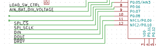
SPI_SS_PIN = P0.6
SPI_MISO_PIN = P0.8
SPI_MOSI_PIN = P0.9
SPI_SCK_PIN = P0.7 

and the schematic showing these pins is: 

I was successfully able to toggle all four pins above, (as well as the RESET P0.21) as GPIOs after I did following: 

1. went to sdk_config.h and changed  NRF_LOG_BACKEND_UART_TX_PIN    to pin 5 instead of 6

2. went to OPTIONS FOR TARGET -> C/C++ -> Preprocessor Symbols -> Define and added " CONFIG_NFCT_PINS_AS_GPIOS" after nrf52382.... and removed the line " CONFIG_GPIO_AS_PINRESET"

But as soon as I run the SPI example code in SDK15 I am unable to toggle these pins and use them as gpios. Especially the SPI_SS_PIN which is pin 6, as soon as I run the SPI code this pin fixes to high value and will not clear/go low.  

My thinking is there something wrong with the way the SPI example configures the spi relevant pins? 

https://devzone.nordicsemi.com/f/nordic-q-a/18546/gpio-not-set-or-clear-with-spi-code this guy seemed to have had the same problem running SPI and with the CS pin...

Thank you! 

Parents
  • Depends perhaps on when you are doing a set/clear test; try setting the SPI_SS_PIN pin to NRF_DRV_SPI_PIN_NOT_USED before initialising the spi, and see if that allows manually set/clear of the /CS pin. Note in this case a manual configuration of the pin to Output must be made as the SPI driver is no longer controlling the pin. The reason for doing this is to ensure nothing else is interfering with the pin; the spi driver does not control the /CS pin with hardware spi but instead runs a set or clear instruction encapsulating the hardware spi transmission. That means the user can just as easily do the set/clear before and after the spi transfer, or allow the handler to do it as in your case.

    Other devices have hardware control over the /CS pin (similar to SCK, MOSI and MISO), but not the nRF52832.

    Also you are probably aware, but if you are testing on a DK then pin 6 is connected in hardware ..

  • Updated:   Now I am configuring the CS pin after I initialize the SPI and it seems to work because the pin goes down to 0.7 V from the earlier Vdd HIGH 3.3V. However, even though the voltage value reduced I do not think this means the SPI_SS_PIN is LOW because the LOW value on my board is typically in millivolts. 

    I am thinking the 0.7V for the CS pin is a floating value. And I do not get why I cannot clear the SPI_SS_PIN?  
    Could this be because the SPI_SS_PIN needs to have a falling edge (and not clear 0) for the SPI peripheral device to be connected? 

    Thanks again

  • Yes, some of my serial uart is enabled. I need to read data from my ADC and send it to the computer via the uart (i.e. I am using NRF_LOG_INFO ). I did change the UART_TX pin number from 6 to 5 in the sdk_config.h file before I even started. That should be okay since pin 5 is unused on my custom board. I am sure pin 6 is not being used anywhere else in the sdk_config.h of my project. Where else should I be checking to make sure where else it is being used? To stop its UART_TX functionality, is removing it from the sdk file enough? 
    P.S. I tried removing all NRF_LOG and LOG initialization code (all the data logging code) in my main file and running the code but the problem persists. 

    My ADS1220 pins are: 
    pin 11 - 3.3V, pin 10 at 5V,    
    Pin 6 and 7 are both at 1.8V.  All the rest of the pins on ADS1220 are as you said should be. 


    Here is my code. What I get from this code is FATAL ERROR on my putty terminal, and I believe the values of the RX and TX registers are showing the addresses of some registers, not data because although these values are persistent (do not change/aren't garbage), they are not corresponding to my voltage data input. 

    /**
     * Copyright (c) 2015 - 2018, Nordic Semiconductor ASA
     *
     * All rights reserved.
     *
     * Redistribution and use in source and binary forms, with or without modification,
     * are permitted provided that the following conditions are met:
     *
     * 1. Redistributions of source code must retain the above copyright notice, this
     *    list of conditions and the following disclaimer.
     *
     * 2. Redistributions in binary form, except as embedded into a Nordic
     *    Semiconductor ASA integrated circuit in a product or a software update for
     *    such product, must reproduce the above copyright notice, this list of
     *    conditions and the following disclaimer in the documentation and/or other
     *    materials provided with the distribution.
     *
     * 3. Neither the name of Nordic Semiconductor ASA nor the names of its
     *    contributors may be used to endorse or promote products derived from this
     *    software without specific prior written permission.
     *
     * 4. This software, with or without modification, must only be used with a
     *    Nordic Semiconductor ASA integrated circuit.
     *
     * 5. Any software provided in binary form under this license must not be reverse
     *    engineered, decompiled, modified and/or disassembled.
     *
     * THIS SOFTWARE IS PROVIDED BY NORDIC SEMICONDUCTOR ASA "AS IS" AND ANY EXPRESS
     * OR IMPLIED WARRANTIES, INCLUDING, BUT NOT LIMITED TO, THE IMPLIED WARRANTIES
     * OF MERCHANTABILITY, NONINFRINGEMENT, AND FITNESS FOR A PARTICULAR PURPOSE ARE
     * DISCLAIMED. IN NO EVENT SHALL NORDIC SEMICONDUCTOR ASA OR CONTRIBUTORS BE
     * LIABLE FOR ANY DIRECT, INDIRECT, INCIDENTAL, SPECIAL, EXEMPLARY, OR
     * CONSEQUENTIAL DAMAGES (INCLUDING, BUT NOT LIMITED TO, PROCUREMENT OF SUBSTITUTE
     * GOODS OR SERVICES; LOSS OF USE, DATA, OR PROFITS; OR BUSINESS INTERRUPTION)
     * HOWEVER CAUSED AND ON ANY THEORY OF LIABILITY, WHETHER IN CONTRACT, STRICT
     * LIABILITY, OR TORT (INCLUDING NEGLIGENCE OR OTHERWISE) ARISING IN ANY WAY OUT
     * OF THE USE OF THIS SOFTWARE, EVEN IF ADVISED OF THE POSSIBILITY OF SUCH DAMAGE.
     *
     */
    #include "nrf_drv_spi.h"
    #include "app_util_platform.h"
    #include "nrf_gpio.h"
    #include "nrf_delay.h"
    #include "boards.h"
    #include "app_error.h"
    #include <string.h>
    #include "nrf_log.h"
    #include "nrf_log_ctrl.h"
    #include "nrf_log_default_backends.h"
    
    #define SPI_INSTANCE  0 /**< SPI instance index. */
    #define S0 21
    #define S1 22
    #define S2 23
    #define S3 24
    #define CS 6
    
    static const nrf_drv_spi_t spi = NRF_DRV_SPI_INSTANCE(SPI_INSTANCE);  /**< SPI instance. */
    static volatile bool spi_xfer_done;  /**< Flag used to indicate that SPI instance completed the transfer. */
    
    
    static uint8_t       m_tx_buf[4];           /**< TX buffer. */
    static uint8_t       m_rx_buf[4];    /**< RX buffer. */
    static const uint8_t tx_length = sizeof(m_tx_buf);        /**< Transfer length. */
    static const uint8_t rx_length = sizeof(m_rx_buf); 
    
    /**
     * @brief SPI user event handler.
     * @param event
     */
    void spi_event_handler(nrf_drv_spi_evt_t const * p_event,
                           void *                    p_context)
    {
        spi_xfer_done = true;
         NRF_LOG_INFO("Transfer completed.");
        //if (m_rx_buf[0] != 1)
        //{
            NRF_LOG_INFO(" Received:");
            NRF_LOG_HEXDUMP_INFO(m_rx_buf, strlen((const char *)m_rx_buf));
    			  nrf_delay_ms(10); 
    			  NRF_LOG_INFO ("Received:  %d  Transmitted:  %d  \n", m_rx_buf, m_tx_buf); 
        //}
    }
    
    
    void init_pins () {
    	
    	nrf_gpio_cfg_output(S0); 
    	nrf_gpio_cfg_output(S1); 
    	nrf_gpio_cfg_output(S2); 
    	nrf_gpio_cfg_output(S3); 
    	 
    	nrf_gpio_pin_set (S3); 
    	nrf_gpio_pin_clear (S1);
    	nrf_gpio_pin_clear (S2);
    	nrf_gpio_pin_set (S0);


    }
    
    int main(void)
    {
       // bsp_board_init(BSP_INIT_LEDS);


        APP_ERROR_CHECK(NRF_LOG_INIT(NULL));
       // NRF_LOG_DEFAULT_BACKENDS_INIT();
    		
    	
    		nrf_delay_ms(50); 
    	
    NRF_LOG_FLUSH();
    	NRF_LOG_INFO ("Hi...");
    	nrf_delay_ms(5); 
        nrf_drv_spi_config_t spi_config = NRF_DRV_SPI_DEFAULT_CONFIG;
        spi_config.miso_pin = SPI_MISO_PIN;
        spi_config.mosi_pin = SPI_MOSI_PIN;
        spi_config.sck_pin  = SPI_SCK_PIN;
    		spi_config.frequency = NRF_DRV_SPI_FREQ_4M; 
    		spi_config.mode     = NRF_DRV_SPI_MODE_1; 
    		//spi_config.irq_priority = APP_IRQ_PRIORITY_HIGHEST;
    	
    		
    		nrf_gpio_cfg_output(SPI_SCK_PIN); 
    		nrf_gpio_cfg_output(SPI_MOSI_PIN);
    		nrf_gpio_cfg_input (SPI_MISO_PIN, NRF_GPIO_PIN_NOPULL); 


        APP_ERROR_CHECK(nrf_drv_spi_init(&spi, &spi_config, spi_event_handler, NULL));
        nrf_delay_ms(20); 


    		nrf_delay_ms(20);
    		init_pins();    // configure CS as output and set it to HIGH 
    
    nrf_gpio_cfg(CS,
                     NRF_GPIO_PIN_DIR_OUTPUT,
                     NRF_GPIO_PIN_INPUT_CONNECT,
                     NRF_GPIO_PIN_NOPULL,
                     NRF_GPIO_PIN_H0H1,
                     NRF_GPIO_PIN_NOSENSE);
    
    //nrf_gpio_cfg_output(CS);
    //nrf_gpio_pin_clear(CS); 
    								 
    		memset(m_tx_buf, 0, tx_length);
    		memset(m_tx_buf, 0, rx_length);
    		m_tx_buf[0] = 0x08;  //START/SYNC HEX COMMAND FOR ADS1220  
    		
    		NRF_LOG_INFO("SPI example started. TX : %d   RX:  %d  \n", m_tx_buf, m_rx_buf);
    	 
    		nrf_gpio_pin_clear(CS); 
    		nrf_delay_ms(1); 
    		APP_ERROR_CHECK(nrf_drv_spi_transfer(&spi, m_tx_buf, tx_length, m_rx_buf, rx_length));
    
            while (!spi_xfer_done)
            {
                __WFE();
            }
    			
    				nrf_delay_ms(10); 


    		memset(m_tx_buf, 0, tx_length);
    		m_tx_buf[0] = 0x08;  //START/SYNC 
    				
        for (;;)
        {
    			
    				
            // Reset rx buffer and transfer done flag
            memset(m_rx_buf, 0, rx_length);
            spi_xfer_done = false;
    				
    				nrf_delay_ms(15); 
    				NRF_LOG_INFO (" Before Transfer , after memset _ rxbuf = %d, txBuf = %d", m_rx_buf[0], m_tx_buf[0]);
    				
            APP_ERROR_CHECK(nrf_drv_spi_transfer(&spi, m_tx_buf, tx_length, m_rx_buf, rx_length));
    
            while (!spi_xfer_done)
            {
                __WFE();
            }
    
            NRF_LOG_FLUSH();
    
            //bsp_board_led_invert(BSP_BOARD_LED_0);
            nrf_delay_ms(800);
    				
    				
        }
    }
    

  • See .\nRF5_SDK_15.2.0_9412b96\components\boards/pca10040.h for the serial port pin definitions using pin 6.

    Fatal Error .. is that coming from an assert()?

    I would suggest moving the following code until after the loop in main; ie logging only when spi_xfer_done is set otherwise the huge delay in that interrupt handler can cause all sorts of issues which will cloud what is going on:

         NRF_LOG_INFO("Transfer completed.");
        //if (m_rx_buf[0] != 1)
        //{
            NRF_LOG_INFO(" Received:");
            NRF_LOG_HEXDUMP_INFO(m_rx_buf, strlen((const char *)m_rx_buf));
    			  nrf_delay_ms(10); 
    			  NRF_LOG_INFO ("Received:  %d  Transmitted:  %d  \n", m_rx_buf, m_tx_buf); 
        //}
    

  • I do not think the FATAL ERROR is because of sending NULL in the spi_transfer() function. I am using the code below (sending a full tx_buf without any NULL but I still get a fatal error). 

    I changed the UART _TX pin from 6 to 26 in the sdk_config.h file and changed the TX_PIN_NUMBER and RX_PIN_NUMBER in the pca10040.h file. But that does not fix the problem. 


    I did manage to pull down PIN 6 (my CS pin) as a GPIO by configuring it in high drive. Pin 6 goes down to 150mV which is a logical 0. But I am still worried because the program still gives me a fatal error and the RX_BUF seems to read a fixed address instead of taking in data from any input.   My rx_buf always contains an int value of "20000006 " no matter what the input. And the tx_buf prints out on the NRF_LOG and int value of "20000002"  even though I am sending "08000000".  I do not understand where the fatal error comes from and why my rx_buf and tx_buf always read these values even when there is no reference to these in the codes? I am using they echo some address... ?

    I am inserting my code here again for reference. 

    /**
     * Copyright (c) 2015 - 2018, Nordic Semiconductor ASA
     *
     * All rights reserved.
     *
     * Redistribution and use in source and binary forms, with or without modification,
     * are permitted provided that the following conditions are met:
     *
     * 1. Redistributions of source code must retain the above copyright notice, this
     *    list of conditions and the following disclaimer.
     *
     * 2. Redistributions in binary form, except as embedded into a Nordic
     *    Semiconductor ASA integrated circuit in a product or a software update for
     *    such product, must reproduce the above copyright notice, this list of
     *    conditions and the following disclaimer in the documentation and/or other
     *    materials provided with the distribution.
     *
     * 3. Neither the name of Nordic Semiconductor ASA nor the names of its
     *    contributors may be used to endorse or promote products derived from this
     *    software without specific prior written permission.
     *
     * 4. This software, with or without modification, must only be used with a
     *    Nordic Semiconductor ASA integrated circuit.
     *
     * 5. Any software provided in binary form under this license must not be reverse
     *    engineered, decompiled, modified and/or disassembled.
     *
     * THIS SOFTWARE IS PROVIDED BY NORDIC SEMICONDUCTOR ASA "AS IS" AND ANY EXPRESS
     * OR IMPLIED WARRANTIES, INCLUDING, BUT NOT LIMITED TO, THE IMPLIED WARRANTIES
     * OF MERCHANTABILITY, NONINFRINGEMENT, AND FITNESS FOR A PARTICULAR PURPOSE ARE
     * DISCLAIMED. IN NO EVENT SHALL NORDIC SEMICONDUCTOR ASA OR CONTRIBUTORS BE
     * LIABLE FOR ANY DIRECT, INDIRECT, INCIDENTAL, SPECIAL, EXEMPLARY, OR
     * CONSEQUENTIAL DAMAGES (INCLUDING, BUT NOT LIMITED TO, PROCUREMENT OF SUBSTITUTE
     * GOODS OR SERVICES; LOSS OF USE, DATA, OR PROFITS; OR BUSINESS INTERRUPTION)
     * HOWEVER CAUSED AND ON ANY THEORY OF LIABILITY, WHETHER IN CONTRACT, STRICT
     * LIABILITY, OR TORT (INCLUDING NEGLIGENCE OR OTHERWISE) ARISING IN ANY WAY OUT
     * OF THE USE OF THIS SOFTWARE, EVEN IF ADVISED OF THE POSSIBILITY OF SUCH DAMAGE.
     *
     */
    #include "nrf_drv_spi.h"
    #include "app_util_platform.h"
    #include "nrf_gpio.h"
    #include "nrf_delay.h"
    #include "boards.h"
    #include "app_error.h"
    #include <string.h>
    #include "nrf_log.h"
    #include "nrf_log_ctrl.h"
    #include "nrf_log_default_backends.h"
    
    #define SPI_INSTANCE  0 /**< SPI instance index. */
    #define S0 21
    #define S1 22
    #define S2 23
    #define S3 24
    #define CS 6
    
    static const nrf_drv_spi_t spi = NRF_DRV_SPI_INSTANCE(SPI_INSTANCE);  /**< SPI instance. */
    static volatile bool spi_xfer_done;  /**< Flag used to indicate that SPI instance completed the transfer. */
    
    
    static uint8_t       m_tx_buf[4];           /**< TX buffer. */
    static uint8_t       m_rx_buf[4];    /**< RX buffer. */
    static const uint8_t tx_length = sizeof(m_tx_buf);        /**< Transfer length. */
    static const uint8_t rx_length = sizeof(m_rx_buf); 
    
    /**
     * @brief SPI user event handler.
     * @param event
     */
    void spi_event_handler(nrf_drv_spi_evt_t const * p_event,
                           void *                    p_context)
    {
        spi_xfer_done = true;
         NRF_LOG_INFO("Transfer completed.");
    			NRF_LOG_HEXDUMP_INFO(m_rx_buf, strlen((const char *)m_rx_buf));
    			  
    			  
    }
    
    
    void init_pins () {
    	
    	nrf_gpio_cfg_output(S0); 
    	nrf_gpio_cfg_output(S1); 
    	nrf_gpio_cfg_output(S2); 
    	nrf_gpio_cfg_output(S3);
    	nrf_gpio_cfg_output(CS); 
    	 
    	nrf_gpio_pin_set (S3); 
    	nrf_gpio_pin_clear (S1);
    	nrf_gpio_pin_clear (S2);
    	nrf_gpio_pin_set (S0);


    }
    
    int main(void)
    {
       // bsp_board_init(BSP_INIT_LEDS);


        APP_ERROR_CHECK(NRF_LOG_INIT(NULL));
       // NRF_LOG_DEFAULT_BACKENDS_INIT();
    		
    	
    NRF_LOG_FLUSH();
    	NRF_LOG_INFO ("Example started: ");
    	nrf_delay_ms(5); 
        nrf_drv_spi_config_t spi_config = NRF_DRV_SPI_DEFAULT_CONFIG;
        spi_config.miso_pin = SPI_MISO_PIN;
        spi_config.mosi_pin = SPI_MOSI_PIN;
        spi_config.sck_pin  = SPI_SCK_PIN;
    		spi_config.frequency = NRF_DRV_SPI_FREQ_1M; 
    		spi_config.mode     = NRF_DRV_SPI_MODE_1; 
    		//spi_config.irq_priority = APP_IRQ_PRIORITY_HIGHEST;
    	
    		
    		nrf_gpio_cfg_output(SPI_SCK_PIN); 
    		nrf_gpio_cfg_output(SPI_MOSI_PIN);
    		nrf_gpio_cfg_input (SPI_MISO_PIN, NRF_GPIO_PIN_NOPULL); 


        APP_ERROR_CHECK(nrf_drv_spi_init(&spi, &spi_config, spi_event_handler, NULL));
        nrf_delay_ms(20); 


    		init_pins();    // configure CS as output and set it to HIGH 
    
    nrf_gpio_cfg(CS,
                     NRF_GPIO_PIN_DIR_OUTPUT,
                     NRF_GPIO_PIN_INPUT_CONNECT,
                     NRF_GPIO_PIN_NOPULL,
                     NRF_GPIO_PIN_H0H1,
                     NRF_GPIO_PIN_NOSENSE);
    
    nrf_delay_ms(10); 
    
    								 
    		memset(m_tx_buf, 0, tx_length);
    		memset(m_tx_buf, 0, rx_length);
    		m_tx_buf[0] = 0x08;  //START/SYNC HEX COMMAND FOR ADS1220  


    		nrf_gpio_pin_clear(CS); 
    
    		APP_ERROR_CHECK(nrf_drv_spi_transfer(&spi, m_tx_buf, tx_length, m_rx_buf, rx_length));
    
            while (!spi_xfer_done)
            {
                __WFE();
            }
    			
    				nrf_delay_ms(10); 


    		memset(m_tx_buf, 0, tx_length);
    		m_tx_buf[0] = 0x08;  //START/SYNC 
    			
    nrf_delay_ms(10); 				
        for (;;)
        {
    			
    				
            // Reset rx buffer and transfer done flag
            memset(m_rx_buf, 0, rx_length);
    				m_tx_buf[0] = 0x08; 
            spi_xfer_done = false;
    				
    				nrf_delay_ms(15); 
    				NRF_LOG_INFO (" Before Transfer , after memset _ rxbuf = %d, txBuf = %d", m_rx_buf[0], m_tx_buf[0]);
    				
            APP_ERROR_CHECK(nrf_drv_spi_transfer(&spi, m_tx_buf, tx_length, m_rx_buf, rx_length));
    
            while (!spi_xfer_done)
            {
                __WFE();
            }
    
            NRF_LOG_FLUSH();
    
            //bsp_board_led_invert(BSP_BOARD_LED_0);
            nrf_delay_ms(800);
    				
    				
        }
    }
    

    Q1: Am I missing some other file where I should disable the other uses of pin P0.6? 
    Q2: I think that forcing the pin 6 down (though successful when I config p6 as high drive) is causing the fatal error. The SPI transfer is not complete or sucessful because my tx and rx buffers read a fixed register value/address ...?
    Q3: Did you use Mode 1 or Mode 0 in your SPI code for ADS1220? 

  • Q1: Depends on what example project you started from; if it was the uart BLE example:

    // pca1004.h
    #define RX_PIN_NUMBER  8
    #define TX_PIN_NUMBER  6
    #define CTS_PIN_NUMBER 7
    #define RTS_PIN_NUMBER 5
    
    // and others confusing the issue ..
    #define SPIS_MISO_PIN   28  // SPI MISO signal.
    #define SPIS_CSN_PIN    12  // SPI CSN signal.
    #define SPIS_MOSI_PIN   25  // SPI MOSI signal.
    #define SPIS_SCK_PIN    29  // SPI SCK signal.
    
    #define SPIM0_SCK_PIN   29  // SPI clock GPIO pin number.
    #define SPIM0_MOSI_PIN  25  // SPI Master Out Slave In GPIO pin number.
    #define SPIM0_MISO_PIN  28  // SPI Master In Slave Out GPIO pin number.
    #define SPIM0_SS_PIN    12  // SPI Slave Select GPIO pin number.
    
    #define SPIM2_SCK_PIN   12  // SPI clock GPIO pin number.
    #define SPIM2_MOSI_PIN  13  // SPI Master Out Slave In GPIO pin number.
    #define SPIM2_MISO_PIN  14  // SPI Master In Slave Out GPIO pin number.
    #define SPIM2_SS_PIN    15  // SPI Slave Select GPIO pin number.
    
    // serialization APPLICATION board - temp. setup for running serialized MEMU tests
    #define SER_APP_RX_PIN              23    // UART RX pin number.
    #define SER_APP_TX_PIN              24    // UART TX pin number.
    #define SER_APP_CTS_PIN             2     // UART Clear To Send pin number.
    #define SER_APP_RTS_PIN             25    // UART Request To Send pin number.
    
    #define SER_APP_SPIM0_SCK_PIN       27     // SPI clock GPIO pin number.
    #define SER_APP_SPIM0_MOSI_PIN      2      // SPI Master Out Slave In GPIO pin number
    #define SER_APP_SPIM0_MISO_PIN      26     // SPI Master In Slave Out GPIO pin number
    #define SER_APP_SPIM0_SS_PIN        23     // SPI Slave Select GPIO pin number
    #define SER_APP_SPIM0_RDY_PIN       25     // SPI READY GPIO pin number
    #define SER_APP_SPIM0_REQ_PIN       24     // SPI REQUEST GPIO pin number
    
    // serialization CONNECTIVITY board
    #define SER_CON_RX_PIN              24    // UART RX pin number.
    #define SER_CON_TX_PIN              23    // UART TX pin number.
    #define SER_CON_CTS_PIN             25    // UART Clear To Send pin number. Not used if HWFC is set to false.
    #define SER_CON_RTS_PIN             2     // UART Request To Send pin number. Not used if HWFC is set to false.
    
    // main.c
    /**@brief  Function for initializing the UART module.
     */
    /**@snippet [UART Initialization] */
    static void uart_init(void)
    {
        uint32_t                     err_code;
        app_uart_comm_params_t const comm_params =
        {
            .rx_pin_no    = RX_PIN_NUMBER,
            .tx_pin_no    = TX_PIN_NUMBER,
            .rts_pin_no   = RTS_PIN_NUMBER,
            .cts_pin_no   = CTS_PIN_NUMBER,
    

    Q2: Is the value you report from the NRF_LOG_INFO or from looking in the debugger?

     .. rxbuf = %d, txBuf = %d", m_rx_buf[0], m_tx_buf[0],

    %d is a 32-bit signed decimal integer, but you really want to display an 8-bit unsigned hex integer so I would suggest replacing %d with %02X. Hex value 0x80 will display as "80". However that is not the issue in the number 0x20000002 (which you would preferably write as 2000:0002 hex); notice 2000:0002 is exactly 4 bytes less than 2000:0006, which is the clue you are looking for. I suggest that 2000:0002 is the starting memory address of your array m_tx_buf[4] and 2000:0006 the address of m_rx_buf[4]. Open a memory window and look at the content of those memory locations to see your actual tx and rx data values, or quicker look at the log output string if available.

    Q3: Equivalent to Mode 1 (it was actually a different mcu); SPI clock low with rising edge shifting data out, clock period 0.5 uSecs, data order MSB first

  • I start with the SPI master example. And I changed the TX pin number in the pca10040.h file and the sdk_config.h file. Do I need to change use of pin 6 anywhere else? 
    Do you have any ideas where the FATAL ERROR is coming from given my code in the above question? 

    I wonder why printing out tx_buf and rx_buf through NRF_LOG_INFO is giving me addresses. 
    Thank you. 

Reply Children
No Data
Related