This post is older than 2 years and might not be relevant anymore
More Info: Consider searching for newer posts

nrf52832 spi (PSEL.SCK)

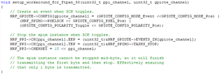
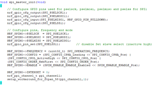
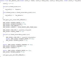
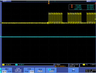
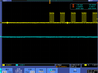
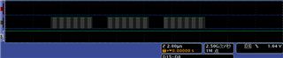
I use nrf52832 SPIM, and I want there are gaps between every 8clock, so I set  NRF_SPIM0->TXD.MAXCNT = 1; NRF_SPIM0->RXD.MAXCNT = 1; ,But there is alway more clock than I want,(I want to write 8clock, but there are 16clock), then the nordic engineer tell me to use PPI(setup_workaround_for_ftpan_58). now, the SPI work well , but I find another question, I must put P0.30 as output pin,and there is gaps between every 8clock, If I didn't config P0.30, there is not gaps between every 8clock, just like bellow,is that right?

I asked the quetion in https://devzone.nordicsemi.com/f/nordic-q-a/40522/nrf52832-spi-psel-sck-timing, but there is no reply.There are more details in the link.

Parents
  • Hi,

    I'm not sure i understand your problem.

    • What do you mean by output pin? The data pin for SPI? A GPIO pin? 
    • What is shown in the picture? The clock signal? The data line?
    • What is meant by not configuring P0.30?

    Best regards

    Jared 

  • the picture is SPI SCK, I want the SPI SCK to have gaps between every 8 clock, so I use NRF_SPIM0->TXD.MAXCNT = 1; NRF_SPIM0->RXD.MAXCNT = 1; 

    P0.30 is an IO, not used as an SPI pin, but I find that , if I not config P0.30 as a output pin, there are not gaps between every 8 clock, just like the picture shows. IF I config P0.30 as a output pin(I config P0.30 like this:nrf_gpio_cfg_output(30); nrf_gpio_pin_clear(30);), there are gaps between every 8 clock just as what I want. 

    the question is :P0.30 is not used as an SPI pin, why it influences the SPI SCK Waveform。the SPI code is just like bellow:

Reply
  • the picture is SPI SCK, I want the SPI SCK to have gaps between every 8 clock, so I use NRF_SPIM0->TXD.MAXCNT = 1; NRF_SPIM0->RXD.MAXCNT = 1; 

    P0.30 is an IO, not used as an SPI pin, but I find that , if I not config P0.30 as a output pin, there are not gaps between every 8 clock, just like the picture shows. IF I config P0.30 as a output pin(I config P0.30 like this:nrf_gpio_cfg_output(30); nrf_gpio_pin_clear(30);), there are gaps between every 8 clock just as what I want. 

    the question is :P0.30 is not used as an SPI pin, why it influences the SPI SCK Waveform。the SPI code is just like bellow:

Children
Related