This post is older than 2 years and might not be relevant anymore
More Info: Consider searching for newer posts

nRF52832 and SHT11 GPIO bit bang

Hello,

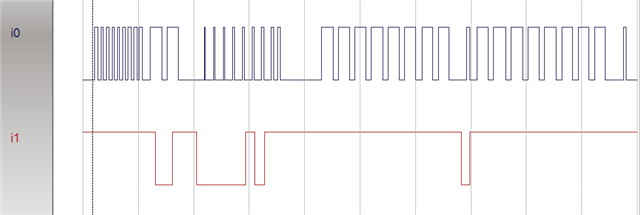
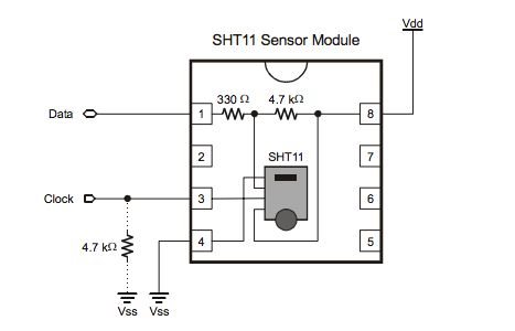
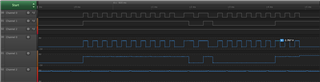
I'm trying to use this code https://github.com/kimyd/SHT1X_on_nrf51822 to communicate with an SHT11 sensor via GPIO pins.  I have a Saleae hooked up an can see the pulses and everything looks okay until the command ACK stage.  The data pin is never pulled low indicating the sensor did not receive the command.  I know the sensor is good as it works find with a RPi using python.

Is there something I need to configure on the GPIO data pin to allow it to be both input and output (I'm just going with S0S1 for the drive).

Any tips/pointers would be greatly appreciated.

Thanks.

Parents
  • Hi,

    Have you compared the logic analyzer trace with the known good sequence you get when using the RPi?

    The SHT11 need a pull up resistor on the DATA line, so you have to enable the internal pull-up resistor in the nRF (unless you have an external pull-up resistor, SHT11 spec states it should be about 10 kΩ). That said, this does not seem to be the problem if the data pin stays always high.

  • Hi Einar,

    Yes, I've compared them and the only difference I can see is that the data line never goes low after the command is entered.  I'm using a Parallax part that has a pull-up integrated (only 4.7K) and I've tried the code with both NOPULL and PULLUP on the input (no difference).  Attached is a scope trace that shows the data line not going low.

    So basically the above is clock on top and data on bottom.  There are 9 pulses with data high (reset), a transmit start sequence and then a code word (5 for humidity). the  ack pulse (9th pulse) does not result in the data line going low. so the rest of the data/clock pulses are basically garbage (all ones).

    The wire diagram shows:

    And this setup works great on a Pi + Python without any additional resistors (don't need the clock pull down).  So I think I'm basically clueless as to how the GPIO pins on the 52832 are supposed to work.  The clock pin is set to output all the time but the data pin flips between input and output.  Is there some special configuration I need to get this to work properly (i.e. is there an extra settle delay when flipping between input and output?).

    Any suggestions would be greatly appreciated.

  • Hi,

    It is a little bit difficult to read the clock and data lines together, but I think i see the same bit pattern you describe. Would it be possible to upload a plot with higher time resolution to make it easier to see the relative timing of the clock and data edges?

    Your description covers about the first half of the graph, and the rest you say is garbage. But the data line is pulled low at one point there, is done by the nRF (your bit ganging SW)?

Reply
  • Hi,

    It is a little bit difficult to read the clock and data lines together, but I think i see the same bit pattern you describe. Would it be possible to upload a plot with higher time resolution to make it easier to see the relative timing of the clock and data edges?

    Your description covers about the first half of the graph, and the rest you say is garbage. But the data line is pulled low at one point there, is done by the nRF (your bit ganging SW)?

Children
  • Hi Einar,

    Here's another capture (maybe better) with some timing ticks

    Some more information:

    I'm using pins 11 & 12 (11 SHT_DATA, 12 SHT_SCK)

    here is the code snipped for writing the command (note TICK, SETTLE and DATA_IN are macros for:

    #define TICK nrf_delay_us(125)

    #define DATA_IN nrf_gpio_cfg(SHT_DATA, NRF_GPIO_PIN_PULLUP)

    #define SETTLE nrf_delay_us(2)

    static char s_write_byte(unsigned char value) { 
      
      unsigned char i,error=0;  
    
      // start trans
      nrf_gpio_cfg_output(SHT_DATA);   
      nrf_gpio_pin_clear(SHT_SCK);                   //Initial state
      nrf_gpio_pin_set(SHT_DATA); 
      TICK;
      nrf_gpio_pin_set(SHT_SCK);
      TICK;
      nrf_gpio_pin_clear(SHT_DATA);
      TICK;
      nrf_gpio_pin_clear(SHT_SCK);  
      TICK; 
      nrf_gpio_pin_set(SHT_SCK);
      TICK;
      nrf_gpio_pin_set(SHT_DATA);		   
      TICK;
      nrf_gpio_pin_clear(SHT_SCK); 
      TICK;
      
      nrf_gpio_pin_clear(SHT_DATA);
      TICK;
    
      //shift bit for masking
      for (i=0x80;i>0;i/=2) { 
        if (i&value) { 
          nrf_gpio_pin_set(SHT_DATA); 
        } else {
          nrf_gpio_pin_clear(SHT_DATA);
        }
    
        nrf_gpio_pin_set(SHT_SCK);   
        TICK;
        nrf_gpio_pin_clear(SHT_SCK);
        TICK;
      }
      
      // release data line
      nrf_gpio_pin_set(SHT_DATA);
      SETTLE;
      
      nrf_gpio_pin_set(SHT_SCK);                            //clk #9 for ack 
      TICK;
      DATA_IN;
      error = nrf_gpio_pin_read(SHT_DATA);	
      nrf_gpio_pin_clear(SHT_SCK);
        
      return error;                     //ack=1 in case of no acknowledge
    }
    

  • Apologies forgot to answer the second part of the question - yes the data line is pulled low on the read by the code.  I changed this so that it never goes to read if it doesn't get the first ack (see 2nd capture).

    I'm use the SEGGER project for the PCA10040 (nRF52832 board) and I've just added the SHT code into the project.  It compiles with no warnings.

  • Hi,

    The new plot was much better Slight smile Can you upload the code which calls your s_write_byte() as well? I am wondering because you wrote that  you write the code word for humidity (000 00101), but it looks to me like you write 000 00111 (Read Status Register). But that does not impact the main issue here, as in any case the SHT11 should have acknowledged by pulling down the data line (according to the datasheet).

    If the data and clock line matches what you get from the RPi, then there is something else preventing the SHT11 from receiving or acking. Is the signal voltage for data and clock at the SHT11 acceptable compared to VDD? Logic '1' should be at least 80% of VDD.

  • Hi Einar,

    Looks like you have identified the 'smoking gun'.  Both my data and clock line are nowhere near 80% of VDD but I have no idea why.  Here are my readings:

    VDD: 4.929V (5V pin on 52832)

    Data Output: 3.436V (you can see it is higher at the end of the trace/picture after I release the data pin)

    Data Input: 2.946V

    Clock Output: 2.767V

    My calculator tells me 80% of 4.929V should be around 3.94V (which is close to data input but not quite).

    Here is a picture:

    Any ideas on how I can raise the voltage levels on Data and Clock to hit 80% VDD (short of a transistor or some kind of relay)?  Given this works on a Pi I'm thinking I need to configure the GPIO pins in some manner.

    Apologies on the code/command mix up.  I've change the code around so many times I mixed up the command order.  The attached image is a: reset, transmission start, read temp command.  

    Thanks,

    Rob.

  • Hi Einar,

    I tried using S0H1 for the output settings but that had little to no effect on the voltage levels I'm seeing (both data and clock outputs are 2.89V.  Out of interest I pulled the SHT out and tried the code which resulted in the same readings both clock and data only reach 2.89V so it's nothing to do with the SHT.

    Doh - okay (I'm a dummy/bit slow), I use VDD instead of the +5V pin and everything looks to be working.  So I guess my questions now is how to re-adjust the GPIO output levels to use +5V? 

Related