This post is older than 2 years and might not be relevant anymore
More Info: Consider searching for newer posts

SPIM3 MOSI, CLK, and D/CX not working as expected after enabling/disabling ArrayList and using PPI and Timer

Hi,

I am using the nRF52840 with no soft device, and I am experiencing an issue with SPIM3 when turning on/off the ArrayList and Shortcut (EVENTS_END and TASKS_START) where the MOSI, CLK, and D/CX lines are not toggling as expected after sending a very large amount of bytes while also using PPI and the Timer Peripherals (following this guide devzone.nordicsemi.com/.../71994 Is there something that I missing here?  Any help would be greatly appreciated!

Here is the sequence that I am issuing:

  1. Initialize SPIM3 module at 32Mbps frequency
    1. Set Config to Active High, Leading clock edge, MSB first
    2. Set Frequency to 32Mbps
    3. Initialize all SCK, MOSI, MISO, CSN, D/CX to High Drive
    4. Set SCK, MOSI, CSN, and D/CX pin to Connected
    5. Set MISO pin to Disconnected
    6. Set IFTIMING.CSNDUR = 3
    7. Set Shortcut to Disabled
    8. Set TX.D List to Disabled
  2. Send several 8-bit commands using SPIM3 to initialize external hardware (D/CX should be low for commands and high for data, automated with SPIM3 peripheral)
    1. Set TXD.PTR, TXD.MAXCNT = 1, RXD.PTR = NULL, RXD.MAXCNT = 0, DCXCNT = 1
    2. Enable the peripheral
    3. Set TASKS_START = 1
    4. Repeat (a) through (c) for several different commands
  3. Set up PPI and Timer2 so that they can be used for the long transmission, but do not enable yet
    1. Timer2
      1. Set mode to Counter
      2. Clear any existing Timer tasks
      3. Set prescaler to 0
      4. Set Bitmode to 16 bit
      5. Enable shortcut to auto-clear when the Compare0 count is reached
      6. Set CC[0] to 4
      7. Enable Compare0 Interrupt
      8. Set Timer2 Priority to 7 and enable Timer2IRQ through NVIC
    2. PPI CH 5
      1. NRF_PPI->CH[5].EEP = (uint32_t) &NRF_SPIM3->EVENTS_END;
      2. NRF_PPI->CH[5].TEP = (uint32_t) &NRF_TIMER2->TASKS_COUNT;
    3. PPI CH 6
      1. NRF_PPI->CH[6].EEP = (uint32_t) &NRF_TIMER2->EVENTS_COMPARE[0];
      2. NRF_PPI->CH[6].TEP = (uint32_t) &NRF_SPIM3->TASKS_STOP;
      3. NRF_PPI->FORK[6].TEP = (uint32_t) &NRF_TIMER2->TASKS_STOP;
  1. Prepare ArrayList prior to long transmission
    1. ArrayList has this structure:


#define BUFFER_SIZE     38400

#define ARRAYLIST_SIZE  5

typedef struct ArrayList

{

     uint8_t buffer[BUFFER_SIZE];

} ArrayList_type;

ArrayList_type Frame_ArrayList[ARRAYLIST_SIZE];

  • Use a For loop to fill every buffer entry with 0xFF for all ArrayList entries (total = 38400 * 5 = 192000 locations filled with 0xFF)
  1. Repeat step 2(a) through 2(c) to send one 8-bit command (D/CX should be low, automated with SPIM3 peripheral)
  2. Enable PPI and Timer2. Then send long transmission using EasyDMA ArrayList with PPI and Timer2 to control when to stop SPIM3
    1. Enable interrupt on Compare0 for Timer2
    2. Start the Timer
    3. Enable PPI for CH5 and CH6
    4. Enable SPIM3 shortcut for EVENTS_END/TASKS_START
    5. Enable TX.D List for ArrayList
    6. Set TXD.PTR to the first entry of the ArrayList[0]
    7. Set TXD.MAXCNT = BUFFERSIZE
    8. Set RXD.PTR = NULL and RXD.MAXCNT = 0
    9. Set DCXCNT = 0
    10. Enable the SPIM3 peripheral and set TASKS_START = 1
  3. The Timer is basically counting after one whole ArrayList is sent (38400 bytes transmitted). Since Timer2 CC[0] = 4, the Timer will send an interrupt after the 4th ArrayList was sent (total 38400 * 4 = 153600 bytes transmitted).
  4. When the Timer2 Interrupt is triggered:
    1. SPIM3 should be stopped and Timer2 should be stopped from the PPI
    2. Disable SPIM3
    3. Clear / disable the Timer2 Interrupt using:
      NRF_TIMER2->INTENCLR = ( TIMER_INTENCLR_COMPARE0_Clear << TIMER_INTENCLR_COMPARE0_Pos );
    4. Clear the Timer2 tasks
    5. Clear the pending IRQ in NVIC for Timer2
    6. Disable shortcut on SPIM3
    7. Disable TXD.List
    8. Disable PPI on CH5 and CH6 using CHENCLR
    9. Repeat step 2(a) through 2(c) to send one 8-bit command (D/CX should be low for the command)


**Everything behaves as expected until step 8(i) where I am experiencing several issues:

  • The SPIM3 module is sending out 18 clock cycles (sometimes more or less) instead of 8 even though I set TXD.MAXCNT = 1
  • The MOSI line is sending out all “0” (MOSI is set up to send 0xAA), and sometimes “0” plus garbage data, and sometimes “0” plus the actual data I intended to send but offset
  • The D/CX line is set to “1” even though I set up DCXCNT = 1


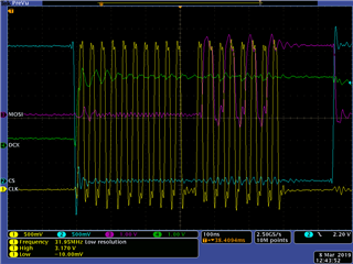
In the above image, this is an example of what I see for step 8(i).  10 clock cycles are sent, followed by 8 additional clocks with MOSI actually being correct but offset by 1 clock.  D/CX is not set low as I intended.

Some interesting discoveries while debugging:

  • If I use the debugger – I set a breakpoint at step 8(i)
    • All the registers for SPIM3, TIMER2, and PPI are set up properly and as expected
      • EVENTS_STOPPED, EVENTS_END, EVENTS_ENDTX, EVENTS_ENDRX, EVENTS_STARTED are all set to “1”
      • SPIM3 shortcut and interrupt were successfully disabled and SPIM3 is currently disabled
      • MAXCNT and TXD.AMOUNT = 0x9600 (as expected since we just finished sending the 38400 bytes and haven’t set up the next 8-bit command yet)
      • PPI is cleared / disabled
    • If I manually step through steps 2(a) through 2(c) using the debugger, then everything behaves properly and works as intended (D/CX is sent properly, the correct command is sent and no extra clocks are sent)
  • If I change BUFFER_SIZE to something smaller, I tried 1000 and 5000 and 10000 instead of 38400, similar behavior is observed, but sometimes the MOSI is eventually able to send what I commanded after 10 clocks of “0” (D/CX still not responding)
  • As a side question, when I set IFTIMING.CSNDUR = 3, I am expecting this to be 46.875ns, but instead I am measuring 80-90ns on the scope. I thought the calculation was 15.625ns * 3 = 46.875ns, but am I missing something?


Thanks for the help!

  • In 8a above SPIM3 Stopped, 8b SPIM3 Disabled. Uh-oh, maybe a step is missing, vis 8a1 SPIM3 Stopped Event:

    The SPI master can be stopped in the middle of a transaction by triggering the STOP task. When triggering the STOP task the SPIM will complete the transmission/reception of the current byte before stopping. A STOPPED event is generated when the SPI master has stopped
    The STOP task may not be always needed (the peripheral might already be stopped), but if it is sent, software shall wait until the STOPPED event was received as a response before disabling the peripheral through the ENABLE register

    Perhaps a suggestion - The 'scope traces above are nice, but would be infinitely better if the probes were adjusted to match the 'scope impedance, usually a tiny screw adjustment on the probe used when connected to the reference Square wave on the 'scope for just that purpose. That would make the waveforms much clearer.

  • Hi,

    I have the PPI set up to automatically trigger the SPIM3 stop command when the Timer2 reaches the Compare0 value of 4. This is in step 3.c.b.  Shouldn't the SPIM3 have already issued TASKS_STOP by step 8A? Thanks

  • Agreed; and I suppose at 32MHz that doesn't take long to happen. However if the STOPPED event confirmation was never generated the code now has no error recovery. Is it possible to see the actual code? Maybe we could replicate the problem.

  • Sure, also as a note, I did try adding TASKS_STOP = 1 for the SPIM3 module at the beginning of the interrupt but didn't have any luck with that.

    Below is the code that I am using.  In our main function, we are performing the following sequence:  initialize all GPIO pins by calling gpio_init, initialize the High Frequency clock by calling init_clocks, call SPIM3_init with 32Mbps frequency, call init_TalonV2, then call fill_screen function.  I didn't include the main() because we also have some other code there that has other functions which aren't used for my testing and didn't want to add confusion.

    // This function initializes the display by sending a few setup commands to the display
    void init_TalonV2(void)
    {
    	// Reset is taken care of by the test menu
    	
    	// Take the display out of sleep mode SLPOUT cmd
    	nrf_delay_ms(120);
    	SPIM3_Command(SLPOUT);
    	nrf_delay_ms(10); // need to delay at least 5ms before starting any other commands
    	
    	// Set up the 16-bit COLMOD command with parameter/data 0x55
    	SPIM3_Command(COLMOD);
    	SPIM3_Data(0x55);
    	nrf_delay_ms(1);
    	
    	// Enable 2-data lane SPI (Data + WRX/DCX)
    	// SPIM3_Command(SPI2EN);
    	// SPIM3_Data(0x10);
    	// nrf_delay_ms(1);
    	
    	// Fill the screen with solid black
    	fill_screen_solid(BLACK);
    	nrf_delay_ms(1);
    	
    	// Send a command to turn on the display DISPON cmd
    	SPIM3_Command(DISPON);
    	nrf_delay_ms(100);
    	
    	test_buzzer_on(); // to simulate PWM current draw at 1kHz
    	
    	// initialize PPI, timer, and frames
    	init_timer();
    	init_PPI();
    	init_solid_frame();
    	
    } // end init_TalonV2
    
    
    //========================================================================================================
    //		void SPIM3_Command(uint8_t com)
    //			- Accepts argument command which contains the command to be sent to the display using 4-line
    //			- DCXCNT should be the number of bytes (8 bits in one byte) in the command, ranging between 0 and 15 (0xF)
    //				- DCX will automatically be set to "0" for the number of bytes specified in DCXCNT and "1" otherwise
    //			- Does not return any value
    //========================================================================================================
    
    void SPIM3_Command(uint8_t com)
    {	
    	NRF_SPIM3->TXD.PTR = (uint32_t)&com;
    	NRF_SPIM3->TXD.MAXCNT = 1;
    	NRF_SPIM3->RXD.PTR = NULL;
    	NRF_SPIM3->RXD.MAXCNT = 0;
    	NRF_SPIM3->DCXCNT = 1; // all display commands are only 8 bits (1 byte) so D/CX should be set to "0"
    	NRF_SPIM3->ENABLE = (SPIM_ENABLE_ENABLE_Enabled << SPIM_ENABLE_ENABLE_Pos);			//enable the peripheral	
    	NRF_SPIM3->TASKS_START = 1;	
    	while(NRF_SPIM3->EVENTS_END == 0)
    	{
    		//wait for transfers to be complete
    	}
    	NRF_SPIM3->EVENTS_END = 0;				//clear event	
    
    	NRF_SPIM3->ENABLE = (SPIM_ENABLE_ENABLE_Disabled << SPIM_ENABLE_ENABLE_Pos);		//disable the peripheral for lowest power consumption when not in use
    } // end SPIM3_Command


    // Initializes one frame of solid white (0xFF)
    void init_solid_frame(void)
    {
    	unsigned int i;
    	for (i = 0; i < BUFFER_SIZE; i++)
    	{
    		Frame_ArrayList[0].buffer[i] = 0xFF;
    		Frame_ArrayList[1].buffer[i] = 0xFF;
    		Frame_ArrayList[2].buffer[i] = 0xFF;
    		Frame_ArrayList[3].buffer[i] = 0xFF;
    		Frame_ArrayList[4].buffer[i] = 0xFF;
    	}
    }


    // This function is called to fill the screen.  Need to send one "RAMWR" command first to tell the display that we want to write to the RAM.  Then we will use EasyDMA to send one frame's worth of data.  Once that is done, the interrupt should trigger so we can send the last "NO_OP" command to the display to tell it that we are done writing to the RAM.
    void fill_screen(unsigned int color)
    {
    	// send RAMWR command
    	SPIM3_Command(RAMWR);
    	
    	// set up peripherals to do a long EasyDMA screen write
    	NRF_TIMER2->INTENSET = ( TIMER_INTENSET_COMPARE0_Set << TIMER_INTENSET_COMPARE0_Pos );
    	NRF_TIMER2->TASKS_START = 1;
    	NRF_PPI->CHENSET = ( (PPI_CHENSET_CH5_Enabled << PPI_CHENSET_CH5_Pos) | (PPI_CHENSET_CH6_Enabled << PPI_CHENSET_CH6_Pos) );
    	NRF_SPIM3->SHORTS = ( SPIM_SHORTS_END_START_Enabled << SPIM_SHORTS_END_START_Pos );
    	NRF_SPIM3->TXD.LIST = ( SPIM_TXD_LIST_LIST_ArrayList << SPIM_TXD_LIST_LIST_Pos );
    	
    	// send 1 frame of data using EasyDMA and the arraylist
    	NRF_SPIM3->TXD.PTR = (uint32_t)&Frame_ArrayList[0];
    	NRF_SPIM3->TXD.MAXCNT = BUFFER_SIZE;
    	NRF_SPIM3->RXD.PTR = NULL;
    	NRF_SPIM3->RXD.MAXCNT = 0;
    	NRF_SPIM3->DCXCNT = 0; // we are only sending data here
    	NRF_SPIM3->ENABLE = (SPIM_ENABLE_ENABLE_Enabled << SPIM_ENABLE_ENABLE_Pos);			//enable the peripheral	
    	NRF_SPIM3->TASKS_START = 1; // eventually the interrupt will trigger and the IRQ handler will be called
    
    } // end fill_screen


    //initialize the SPIM3 peripheral 
    void SPIM3_init(volatile uint32_t spi_mbps)
    {
    	//peripheral configuration - set up as Mode 0 because the display samples at leading, rising edge of clock
    	NRF_SPIM3->CONFIG 		= ((SPIM_CONFIG_CPOL_ActiveHigh << SPIM_CONFIG_CPOL_Pos) | (SPIM_CONFIG_CPHA_Leading << SPIM_CONFIG_CPHA_Pos) | (SPIM_CONFIG_ORDER_MsbFirst << SPIM_CONFIG_ORDER_Pos));
    	NRF_SPIM3->FREQUENCY 	= (spi_mbps << SPIM_FREQUENCY_FREQUENCY_Pos);
    
    	//pin initialization
    	NRF_SPIM3->PSEL.SCK 	= ((SPIM_PSEL_SCK_CONNECT_Connected << SPIM_PSEL_SCK_CONNECT_Pos) | (PIN_SPI_CLK << SPIM_PSEL_SCK_PIN_Pos));
    	NRF_SPIM3->PSEL.MOSI 	= ((SPIM_PSEL_MOSI_CONNECT_Connected << SPIM_PSEL_MOSI_CONNECT_Pos) | (PIN_SPI_MOSI << SPIM_PSEL_MOSI_PIN_Pos));
    	NRF_SPIM3->PSEL.MISO  = ((SPIM_PSEL_MISO_CONNECT_Disconnected << SPIM_PSEL_MISO_CONNECT_Pos)); // plan to not read anything from the display and only write to display
    	if (SPI_3LINE == 0) // we have 4-line serial so this will be connected
    	{ 
    		NRF_SPIM3->PSEL.CSN   = ((SPIM_PSEL_CSN_CONNECT_Connected << SPIM_PSEL_CSN_CONNECT_Pos) | (PIN_SPI_SS << SPIM_PSEL_CSN_PIN_Pos));
    		NRF_SPIM3->CSNPOL     = ( SPIM_CSNPOL_CSNPOL_LOW << SPIM_CSNPOL_CSNPOL_Pos );
    	}
    	NRF_SPIM3->PSELDCX    = ((SPIM_PSELDCX_CONNECT_Connected << SPIM_PSELDCX_CONNECT_Pos) | (PIN_SPI_MISO << SPIM_PSELDCX_PIN_Pos) );
    	
    	// new
    	NRF_SPIM3->IFTIMING.CSNDUR = ( 3 << SPIM_IFTIMING_CSNDUR_CSNDUR_Pos ); // 3*15.625ns = 46.875ns
    	NRF_SPIM3->SHORTS = ( SPIM_SHORTS_END_START_Disabled << SPIM_SHORTS_END_START_Pos );
    	NRF_SPIM3->TXD.LIST = ( SPIM_TXD_LIST_LIST_Disabled << SPIM_TXD_LIST_LIST_Pos );
    } // end SPIM3_init


    // This function initializes the two PPI channels required to automate a very long EasyDMA SPIM3 transaction
    void init_PPI(void)
    {
    	NRF_PPI->CH[5].EEP = (uint32_t) &NRF_SPIM3->EVENTS_END; // probably could be more specific and put EVENTS_ENDTX
    	NRF_PPI->CH[5].TEP = (uint32_t) &NRF_TIMER2->TASKS_COUNT;
    	
    	NRF_PPI->CH[6].EEP = (uint32_t) &NRF_TIMER2->EVENTS_COMPARE[0];
    	NRF_PPI->CH[6].TEP = (uint32_t) &NRF_SPIM3->TASKS_STOP;
    	NRF_PPI->FORK[6].TEP = (uint32_t) &NRF_TIMER2->TASKS_STOP;
    }


    // This function initializes the Timer peripheral as a counter and enables the interrupt when Compare0 occurs
    void init_timer(void)
    {
    	// set up timer mode
    	NRF_TIMER2->MODE = (TIMER_MODE_MODE_Counter << TIMER_MODE_MODE_Pos); // timer mode (rather than counter mode) requires a manual start and stop of the timer
    	
    	// clear any existing timer tasks
    	NRF_TIMER2->TASKS_CLEAR = 1;
    	
    	// set timer prescaler, 16MHz / (2^prescaler)
    	NRF_TIMER2->PRESCALER = 0;
    	
    	// sets the timer's maximum value
    	NRF_TIMER2->BITMODE = ( TIMER_BITMODE_BITMODE_16Bit << TIMER_BITMODE_BITMODE_Pos );
    	
    	// sets up a shortcut to auto-clear the timer when the compare count is reached
    	NRF_TIMER2->SHORTS = ( TIMER_SHORTS_COMPARE0_CLEAR_Enabled << TIMER_SHORTS_COMPARE0_CLEAR_Pos );
    	NRF_TIMER2->CC[0] = 4;
    	NRF_TIMER2->INTENSET = ( TIMER_INTENSET_COMPARE0_Set << TIMER_INTENSET_COMPARE0_Pos );
    	
    	NVIC_SetPriority(TIMER2_IRQn, 7);
    	NVIC_EnableIRQ(TIMER2_IRQn);
    }


    // This code should be called when the Timer2 interrupt is triggered
    void TIMER2_IRQHandler(void)
    {	
    	NRF_SPIM3->TASKS_STOP = 1; // I just added this per suggestion from Nordic, but did not see any change with this code here
    
    	// disable PPI, SPIM3 module, and shortcut/arraylist in order to send one SPIM3 No-op command normally
    	NRF_SPIM3->ENABLE = (SPIM_ENABLE_ENABLE_Disabled << SPIM_ENABLE_ENABLE_Pos);		//disable the peripheral for lowest power consumption when not in use
    	
    	// Clear interrupt
    	NRF_TIMER2->TASKS_STOP = 1;
    	NRF_TIMER2->INTENCLR = ( TIMER_INTENCLR_COMPARE0_Clear << TIMER_INTENCLR_COMPARE0_Pos );
    	NRF_TIMER2->TASKS_CLEAR = 1;
    	NVIC_ClearPendingIRQ(TIMER2_IRQn);
    	
    	NRF_SPIM3->SHORTS = ( SPIM_SHORTS_END_START_Disabled << SPIM_SHORTS_END_START_Pos );
    	NRF_SPIM3->TXD.LIST = ( SPIM_TXD_LIST_LIST_Disabled << SPIM_TXD_LIST_LIST_Pos );
    	
    	NRF_PPI->CHENCLR = ( (PPI_CHENCLR_CH5_Clear << PPI_CHENCLR_CH5_Pos) | (PPI_CHENCLR_CH6_Clear << PPI_CHENCLR_CH6_Pos) );
    	
    	// Send No-op command to tell the display we are done writing to the RAM
    	SPIM3_Command(0xAA);	
    }

    //========================================================================================================
    //		void gpio_init(void)
    //			- Initializes and configures all GPIO pins
    //			- Standard drive is good for low current and slow signals
    //			- High drive is for fast signals and high current
    //			- Does not return any value
    //========================================================================================================
    void gpio_init(void)
    {
    	// Peripheral Pin configurations
    	gpio_pin_cnf( PIN_RED_CONTROL, 
    		( GPIO_PIN_CNF_DIR_Output << GPIO_PIN_CNF_DIR_Pos ) |
    		( GPIO_PIN_CNF_INPUT_Disconnect << GPIO_PIN_CNF_INPUT_Pos ) |
    		( GPIO_PIN_CNF_PULL_Disabled << GPIO_PIN_CNF_PULL_Pos ) |
    		( GPIO_PIN_CNF_DRIVE_S0S1 << GPIO_PIN_CNF_DRIVE_Pos ) |
    		( GPIO_PIN_CNF_SENSE_Disabled << GPIO_PIN_CNF_SENSE_Pos ) 
    	);
    
    	gpio_pin_cnf( PIN_GREEN_CONTROL, 
    		( GPIO_PIN_CNF_DIR_Output << GPIO_PIN_CNF_DIR_Pos ) |
    		( GPIO_PIN_CNF_INPUT_Disconnect << GPIO_PIN_CNF_INPUT_Pos ) |
    		( GPIO_PIN_CNF_PULL_Disabled << GPIO_PIN_CNF_PULL_Pos ) |
    		( GPIO_PIN_CNF_DRIVE_S0S1 << GPIO_PIN_CNF_DRIVE_Pos ) |
    		( GPIO_PIN_CNF_SENSE_Disabled << GPIO_PIN_CNF_SENSE_Pos ) 
    	);
    
    	gpio_pin_cnf( PIN_BLUE_CONTROL, 
    		( GPIO_PIN_CNF_DIR_Output << GPIO_PIN_CNF_DIR_Pos ) |
    		( GPIO_PIN_CNF_INPUT_Disconnect << GPIO_PIN_CNF_INPUT_Pos ) |
    		( GPIO_PIN_CNF_PULL_Disabled << GPIO_PIN_CNF_PULL_Pos ) |
    		( GPIO_PIN_CNF_DRIVE_S0S1 << GPIO_PIN_CNF_DRIVE_Pos ) |
    		( GPIO_PIN_CNF_SENSE_Disabled << GPIO_PIN_CNF_SENSE_Pos ) 
    	);
    
    	gpio_pin_cnf( PIN_BUZZER, 
    		( GPIO_PIN_CNF_DIR_Output << GPIO_PIN_CNF_DIR_Pos ) |
    		( GPIO_PIN_CNF_INPUT_Disconnect << GPIO_PIN_CNF_INPUT_Pos ) |
    		( GPIO_PIN_CNF_PULL_Disabled << GPIO_PIN_CNF_PULL_Pos ) |
    		( GPIO_PIN_CNF_DRIVE_S0S1 << GPIO_PIN_CNF_DRIVE_Pos ) |
    		( GPIO_PIN_CNF_SENSE_Disabled << GPIO_PIN_CNF_SENSE_Pos ) 
    	);	
    	
    	// Configure TRF7970A
    	gpio_pin_cnf( PIN_NFC_EN, 
    		( GPIO_PIN_CNF_DIR_Output << GPIO_PIN_CNF_DIR_Pos ) |
    		( GPIO_PIN_CNF_INPUT_Disconnect << GPIO_PIN_CNF_INPUT_Pos ) |
    		( GPIO_PIN_CNF_PULL_Disabled << GPIO_PIN_CNF_PULL_Pos ) |
    		( GPIO_PIN_CNF_DRIVE_S0S1 << GPIO_PIN_CNF_DRIVE_Pos ) |
    		( GPIO_PIN_CNF_SENSE_Disabled << GPIO_PIN_CNF_SENSE_Pos ) 
    	);
    	
    	gpio_pin_cnf( PIN_NFC_EN2, 
    		( GPIO_PIN_CNF_DIR_Output << GPIO_PIN_CNF_DIR_Pos ) |
    		( GPIO_PIN_CNF_INPUT_Disconnect << GPIO_PIN_CNF_INPUT_Pos ) |
    		( GPIO_PIN_CNF_PULL_Disabled << GPIO_PIN_CNF_PULL_Pos ) |
    		( GPIO_PIN_CNF_DRIVE_S0S1 << GPIO_PIN_CNF_DRIVE_Pos ) |
    		( GPIO_PIN_CNF_SENSE_Disabled << GPIO_PIN_CNF_SENSE_Pos ) 
    	);
    
    	gpio_pin_cnf( PIN_MOD, 
    		( GPIO_PIN_CNF_DIR_Output << GPIO_PIN_CNF_DIR_Pos ) |
    		( GPIO_PIN_CNF_INPUT_Disconnect << GPIO_PIN_CNF_INPUT_Pos ) |
    		( GPIO_PIN_CNF_PULL_Disabled << GPIO_PIN_CNF_PULL_Pos ) |
    		( GPIO_PIN_CNF_DRIVE_S0S1 << GPIO_PIN_CNF_DRIVE_Pos ) |
    		( GPIO_PIN_CNF_SENSE_Disabled << GPIO_PIN_CNF_SENSE_Pos ) 
    	);
    	
    	gpio_pin_cnf( PIN_ASKOOK, 
    		( GPIO_PIN_CNF_DIR_Output << GPIO_PIN_CNF_DIR_Pos ) |
    		( GPIO_PIN_CNF_INPUT_Disconnect << GPIO_PIN_CNF_INPUT_Pos ) |
    		( GPIO_PIN_CNF_PULL_Disabled << GPIO_PIN_CNF_PULL_Pos ) |
    		( GPIO_PIN_CNF_DRIVE_S0S1 << GPIO_PIN_CNF_DRIVE_Pos ) |
    		( GPIO_PIN_CNF_SENSE_Disabled << GPIO_PIN_CNF_SENSE_Pos ) 
    	);
    	
    	gpio_pin_cnf( PIN_IRQ,
    		( GPIO_PIN_CNF_DIR_Input << GPIO_PIN_CNF_DIR_Pos ) |
    		( GPIO_PIN_CNF_INPUT_Connect << GPIO_PIN_CNF_INPUT_Pos ) |
    		( GPIO_PIN_CNF_PULL_Pullup << GPIO_PIN_CNF_PULL_Pos ) |
    		( GPIO_PIN_CNF_DRIVE_S0S1 << GPIO_PIN_CNF_DRIVE_Pos ) |
    		( GPIO_PIN_CNF_SENSE_Disabled << GPIO_PIN_CNF_SENSE_Pos ) 
    	);
    
    	gpio_pin_cnf( PIN_SPI_SS, 
    		( GPIO_PIN_CNF_DIR_Output << GPIO_PIN_CNF_DIR_Pos ) |
    		( GPIO_PIN_CNF_INPUT_Disconnect << GPIO_PIN_CNF_INPUT_Pos ) |
    		( GPIO_PIN_CNF_PULL_Disabled << GPIO_PIN_CNF_PULL_Pos ) |
    		( GPIO_PIN_CNF_DRIVE_H0H1 << GPIO_PIN_CNF_DRIVE_Pos ) |
    		( GPIO_PIN_CNF_SENSE_Disabled << GPIO_PIN_CNF_SENSE_Pos ) 
    	);
    	
    	gpio_pin_cnf( PIN_RESET,
    		( GPIO_PIN_CNF_DIR_Input << GPIO_PIN_CNF_DIR_Pos ) |
    		( GPIO_PIN_CNF_INPUT_Connect << GPIO_PIN_CNF_INPUT_Pos ) |
    		( GPIO_PIN_CNF_PULL_Pullup << GPIO_PIN_CNF_PULL_Pos ) |
    		( GPIO_PIN_CNF_DRIVE_S0S1 << GPIO_PIN_CNF_DRIVE_Pos ) |
    		( GPIO_PIN_CNF_SENSE_Disabled << GPIO_PIN_CNF_SENSE_Pos ) 
    	);
    
    	// Configure SPI Master 0 with default values before enabling SPI peripheral
    	gpio_pin_cnf( PIN_SPI_CLK,
    		( GPIO_PIN_CNF_DIR_Output << GPIO_PIN_CNF_DIR_Pos ) |
    		( GPIO_PIN_CNF_INPUT_Disconnect << GPIO_PIN_CNF_INPUT_Pos ) |
    		( GPIO_PIN_CNF_PULL_Disabled << GPIO_PIN_CNF_PULL_Pos ) |
    		( GPIO_PIN_CNF_DRIVE_H0H1 << GPIO_PIN_CNF_DRIVE_Pos ) |
    		( GPIO_PIN_CNF_SENSE_Disabled << GPIO_PIN_CNF_SENSE_Pos ) 
    	);
    	
    	gpio_pin_cnf( PIN_SPI_MOSI,
    		( GPIO_PIN_CNF_DIR_Output << GPIO_PIN_CNF_DIR_Pos ) |
    		( GPIO_PIN_CNF_INPUT_Disconnect << GPIO_PIN_CNF_INPUT_Pos ) |
    		( GPIO_PIN_CNF_PULL_Disabled << GPIO_PIN_CNF_PULL_Pos ) |
    		( GPIO_PIN_CNF_DRIVE_H0H1 << GPIO_PIN_CNF_DRIVE_Pos ) |
    		( GPIO_PIN_CNF_SENSE_Disabled << GPIO_PIN_CNF_SENSE_Pos ) 
    	);
    	
    	gpio_pin_cnf( PIN_SPI_MISO,
    		( GPIO_PIN_CNF_DIR_Input << GPIO_PIN_CNF_DIR_Pos ) |
    		( GPIO_PIN_CNF_INPUT_Connect << GPIO_PIN_CNF_INPUT_Pos ) |
    		( GPIO_PIN_CNF_PULL_Disabled << GPIO_PIN_CNF_PULL_Pos ) |
    		( GPIO_PIN_CNF_DRIVE_H0H1 << GPIO_PIN_CNF_DRIVE_Pos ) | 
    		( GPIO_PIN_CNF_SENSE_Disabled << GPIO_PIN_CNF_SENSE_Pos )  
    	);
    
    	// Configure SPI Slave 1 with default values before enabling SPI peripheral
    	gpio_pin_cnf( PIN_MX_SENFRM,
    		( GPIO_PIN_CNF_DIR_Input << GPIO_PIN_CNF_DIR_Pos ) |
    		( GPIO_PIN_CNF_INPUT_Connect << GPIO_PIN_CNF_INPUT_Pos ) |
    		( GPIO_PIN_CNF_PULL_Disabled << GPIO_PIN_CNF_PULL_Pos ) |
    		( GPIO_PIN_CNF_DRIVE_H0H1 << GPIO_PIN_CNF_DRIVE_Pos ) |
    		( GPIO_PIN_CNF_SENSE_Disabled << GPIO_PIN_CNF_SENSE_Pos ) 
    	);
    	
    	gpio_pin_cnf( PIN_MX_SENCLK,
    		( GPIO_PIN_CNF_DIR_Input << GPIO_PIN_CNF_DIR_Pos ) |
    		( GPIO_PIN_CNF_INPUT_Connect << GPIO_PIN_CNF_INPUT_Pos ) |
    		( GPIO_PIN_CNF_PULL_Disabled << GPIO_PIN_CNF_PULL_Pos ) |
    		( GPIO_PIN_CNF_DRIVE_H0H1 << GPIO_PIN_CNF_DRIVE_Pos ) |
    		( GPIO_PIN_CNF_SENSE_Disabled << GPIO_PIN_CNF_SENSE_Pos ) 
    	);
    	
    	gpio_pin_cnf( PIN_MX_SENOUT,
    		( GPIO_PIN_CNF_DIR_Input << GPIO_PIN_CNF_DIR_Pos ) |
    		( GPIO_PIN_CNF_INPUT_Connect << GPIO_PIN_CNF_INPUT_Pos ) |
    		( GPIO_PIN_CNF_PULL_Disabled << GPIO_PIN_CNF_PULL_Pos ) |
    		( GPIO_PIN_CNF_DRIVE_H0H1 << GPIO_PIN_CNF_DRIVE_Pos ) |
    		( GPIO_PIN_CNF_SENSE_Disabled << GPIO_PIN_CNF_SENSE_Pos ) 
    	);
    	
    	gpio_pin_cnf( PIN_MX_SENIN,
    		( GPIO_PIN_CNF_DIR_Output << GPIO_PIN_CNF_DIR_Pos ) |
    		( GPIO_PIN_CNF_INPUT_Disconnect << GPIO_PIN_CNF_INPUT_Pos ) |
    		( GPIO_PIN_CNF_PULL_Disabled << GPIO_PIN_CNF_PULL_Pos ) |
    		( GPIO_PIN_CNF_DRIVE_H0H1 << GPIO_PIN_CNF_DRIVE_Pos ) | // high drive for MISO only GPIO_PIN_CNF_DRIVE_H0H1
    		( GPIO_PIN_CNF_SENSE_Disabled << GPIO_PIN_CNF_SENSE_Pos )  
    	);
    	
    	
    	// initialize PIN_TEST as a GPIO
    		gpio_pin_cnf( PIN_TEST,
    		( GPIO_PIN_CNF_DIR_Output << GPIO_PIN_CNF_DIR_Pos ) |
    		( GPIO_PIN_CNF_INPUT_Disconnect << GPIO_PIN_CNF_INPUT_Pos ) |
    		( GPIO_PIN_CNF_PULL_Disabled << GPIO_PIN_CNF_PULL_Pos ) |
    		( GPIO_PIN_CNF_DRIVE_S0S1 << GPIO_PIN_CNF_DRIVE_Pos ) | 
    		( GPIO_PIN_CNF_SENSE_Disabled << GPIO_PIN_CNF_SENSE_Pos )  
    	);
    	
    	// Pin initial settings
    	gpio_pin_clear(PIN_RED_CONTROL); 
    	gpio_pin_clear(PIN_GREEN_CONTROL);
    	gpio_pin_clear(PIN_BLUE_CONTROL); 
    	gpio_pin_clear(PIN_BUZZER); 
    	
    	gpio_pin_clear(PIN_NFC_EN);
    	gpio_pin_clear(PIN_NFC_EN2);
    	gpio_pin_clear(PIN_MOD);
    	gpio_pin_set(PIN_ASKOOK);
    	
    	// initial values for display
    	gpio_pin_clear(PIN_SPI_MOSI);
    	gpio_pin_clear(PIN_SPI_CLK);
    	gpio_pin_clear(PIN_SPI_MISO);
    	gpio_pin_set(PIN_TEST); // used as Display Reset
    	slaveSelectHigh();
    	
    } // end gpio_init


    //========================================================================================================
    //		static void init_clocks(void)
    //			- Initializes and configures the NRF high frequency clock
    //			- Does not return any value
    //========================================================================================================
    
    static void init_clocks(void)
    {
    	// Start high frequency clock off crystal
    	NRF_CLOCK->TASKS_HFCLKSTART = 1;							//start high frequency oscillator off external crystal source
    	while (NRF_CLOCK->EVENTS_HFCLKSTARTED == 0)		//wait for confirmation that HFOSC has started	
      {
    		//Wait for HFCLK to start
      }
    	NRF_CLOCK->EVENTS_HFCLKSTARTED = 0; 					//Clear event
    } // end init_clocks()


  • Oops I forgot to include some defines:

    #define NOP_CMD         0x00
    #define SLPOUT          0x11
    #define DISPON          0x29
    #define RAMWR           0x2C
    #define COLMOD          0x3A
    #define SPI2EN          0xE7
    #define WHITE           0xFFFF
    #define BLACK           0x0000
    #define SPI_3LINE       0x0 // 0 is 4-line, 1 is 3-line

Related