
According to the nRF51822 PS v3.1, table 51, offset error for the internal ADC is up to 2% and the gain error can be up to 2%. Is it possible to correct this error to obtain better accuracy for the ADC?
According to the nRF51822 PS v3.1, table 51, offset error for the internal ADC is up to 2% and the gain error can be up to 2%. Is it possible to correct this error to obtain better accuracy for the ADC?
The offset and gain error is different from IC to IC and may therefore be calibrated for each IC to obtain acceptable accuracy. On nRF51 third revision IC's the offset and gain error has been measured and written into non-volatile memory for 10-bit ADC resolution, see update on this thread from 10.4.2015. To otherwise generally correct the offset and gain error, perform the following steps:
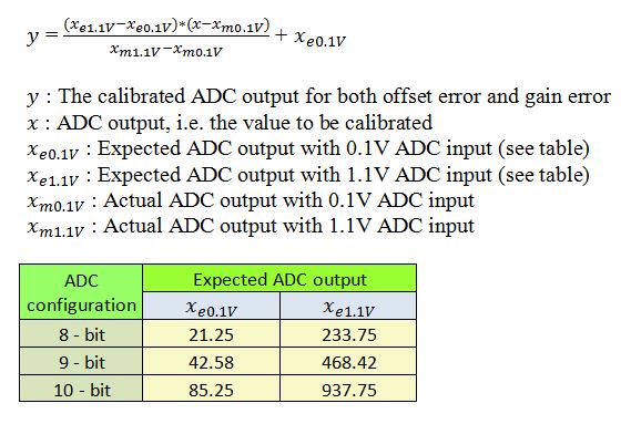
The transfer function is:
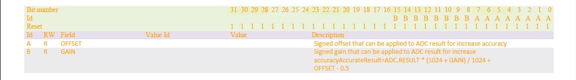
Update 10.4.2015 An easier way to apply ADC calibration for third revision nRF51 is to read the gain error and offset error numbers available in memory address 0x10000024. This information is not available for first or second nRF51 revision ICs. For third revision nRF51 devices, the offset and gain error values have been measured for each nRF51 chip after production and have been written to memory address 0x10000024. The register at this memory address is listed below and the gain error and offset error values are valid for 10-bit sampling only. For 8-bit and 9-bit sampling, there are no values available:
The ADC offset and gain error are read with the following command:
nrfjprog --memrd 0x10000024 --n 4
If e.g. the perceived value is "0x10000024: FFFF0102" then GAIN_ERROR=1 and OFFSET_ERROR=2.
The offset and gain values are two's complement numbers. This means that if e.g. the observed value is 0xFFFF03FF, then GAIN_ERROR=3 and OFFSET_ERROR=-1
Similarly, if the observed value is 0xFFFFFEFC, then GAIN_ERROR=-2 and OFFSET_ERROR=-3
The calibrated value y is obtained for 10-bit ADC sample x with:
y = x * (1024+GAIN_ERROR) / 1024 + OFFSET_ERROR - 0.5
where 0.5 LSB is subtracted to compensate for ADC quantization error.
Update 27.10.2015
To obtain the offset error and gain error at runtime the FICR value can be read with:
	static uint32_t ficr_value_32;
	static int8_t offset_error;
	static int8_t gain_error;

	ficr_value_32 = *(uint32_t*)0x10000024;
	offset_error = ficr_value_32;
	gain_error = ficr_value_32 >> 8;
The offset and gain error is different from IC to IC and may therefore be calibrated for each IC to obtain acceptable accuracy. On nRF51 third revision IC's the offset and gain error has been measured and written into non-volatile memory for 10-bit ADC resolution, see update on this thread from 10.4.2015. To otherwise generally correct the offset and gain error, perform the following steps:
The transfer function is:
Update 10.4.2015 An easier way to apply ADC calibration for third revision nRF51 is to read the gain error and offset error numbers available in memory address 0x10000024. This information is not available for first or second nRF51 revision ICs. For third revision nRF51 devices, the offset and gain error values have been measured for each nRF51 chip after production and have been written to memory address 0x10000024. The register at this memory address is listed below and the gain error and offset error values are valid for 10-bit sampling only. For 8-bit and 9-bit sampling, there are no values available:
The ADC offset and gain error are read with the following command:
nrfjprog --memrd 0x10000024 --n 4
If e.g. the perceived value is "0x10000024: FFFF0102" then GAIN_ERROR=1 and OFFSET_ERROR=2.
The offset and gain values are two's complement numbers. This means that if e.g. the observed value is 0xFFFF03FF, then GAIN_ERROR=3 and OFFSET_ERROR=-1
Similarly, if the observed value is 0xFFFFFEFC, then GAIN_ERROR=-2 and OFFSET_ERROR=-3
The calibrated value y is obtained for 10-bit ADC sample x with:
y = x * (1024+GAIN_ERROR) / 1024 + OFFSET_ERROR - 0.5
where 0.5 LSB is subtracted to compensate for ADC quantization error.
Update 27.10.2015
To obtain the offset error and gain error at runtime the FICR value can be read with:
	static uint32_t ficr_value_32;
	static int8_t offset_error;
	static int8_t gain_error;

	ficr_value_32 = *(uint32_t*)0x10000024;
	offset_error = ficr_value_32;
	gain_error = ficr_value_32 >> 8;

Stephan, which document contains the above table with the offset and gain error values at offset 0x0024 of the FICR?

Hi Philip
There is unfortunately no official document that contains this information. This information is made public only here on this thread. At this point I am not sure for the reasons for it not to be in official documentation but perhaps because it is limited information, since it only applies for 10 bit sampling. If this information will be in official documentation it will be in a future release of the nRF51 Series Reference Manual.

Very useful info. Two related questions:
Why that "-0.5" in the formula? I have an example (yours I guess) where that value is ommited.
Is there any way we can automatically read this calibration value from code? For example a function that only runs once at the beggining, or similar. So we don't have to manually get the value with nrfjprog. Thanks
Hi stefan, Does the nRF52840 have a memory address that can be read the gain error and offset error numbers for ADC calibration?
The above sample code doesn't look good to me. I suspect it falls to the 3rd case below.
C99 6.3.1.3 Signed and unsigned integers
When a value with integer type is converted to another integer type other than _Bool, if the value can be represented by the new type, it is unchanged.
Otherwise, if the new type is unsigned, the value is converted by repeatedly adding or subtracting one more than the maximum value that can be represented in the new type until the value is in the range of the new type.49)
Otherwise, the new type is signed and the value cannot be represented in it; either the result is implementation-defined or an implementation-defined signal is raised.
A proposed alternative:
int8_t offset_error = *(int8_t*)0x10000024;
int8_t gain_error = *(int8_t*)0x10000025;