This post is older than 2 years and might not be relevant anymore
More Info: Consider searching for newer posts

ADS1299 reading register_SPI_nRF52832

Hello everyone,

Testing on:

  • nRF52DK (PCA 10040)
  • SDK 13.0.0

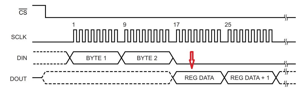
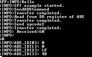
I have been struggling with reading from the register of ADS1299. I just want to try to read info from ID register of this IC to make sure getting correctly data using SPI.

Below is my code to read the register, I couldn't receive correct the data which is supposed to get 0x1E. Could you help me to check whether something is wrong in this code?

Thank you!

uint8_t RREG_ADS(uint8_t address)
{
	  uint8_t data_reg;
	  dataToSend[0] = address | 0x20;  //Opcode 000n nnnn =0 : write n channels
	  nrf_gpio_pin_clear(SPIM0_SS_PIN); // enable SS pin for ADS
	  if(DEBUG){NRF_LOG_INFO("Read from DR register of ADS\r\n");NRF_LOG_FLUSH();}
	  // Reset rx buffer and transfer done flag
	  spi_xfer_done = false; memset(m_rx_buf,0,sizeof(m_rx_buf));
      APP_ERROR_CHECK(nrf_drv_spi_transfer(&spi, dataToSend, 1, &data_reg, 1));
	  while (!spi_xfer_done){__WFE();}
	  NRF_LOG_FLUSH();
	  if(DEBUG){NRF_LOG_INFO("Send 0x00\r\n");NRF_LOG_FLUSH();}
	  spi_xfer_done = false; memset(m_rx_buf,0,sizeof(m_rx_buf));
	  APP_ERROR_CHECK(nrf_drv_spi_transfer(&spi, 0x00, 1, m_rx_buf, sizeof(m_rx_buf)));  
	  while (!spi_xfer_done){__WFE();}
	  NRF_LOG_FLUSH();
	  nrf_gpio_pin_set(SPIM0_SS_PIN); // disable SS pin for ADS
		nrf_delay_us(15);
		return data_reg;	
}

Parents
  • Hi all,

    I modified my code a bit.

    uint8_t* RREG_ADS(uint8_t address)
    {
    		static uint8_t data_reg[4];
    		dataToSend[0] = address | 0x20;				//Opcode 000n nnnn =0 : write n channels
    		uint8_t opcode2 = 0x00;  // specify how many registers used
    	  nrf_gpio_pin_clear(CS); // enable SS pin for ADS
    	  if(DEBUG){NRF_LOG_INFO("Read from DR register of ADS\r\n");NRF_LOG_FLUSH();}
    	  // Reset rx buffer and transfer done flag
    	  spi_xfer_done = false; memset(data_reg,0,sizeof(data_reg));
          APP_ERROR_CHECK(nrf_drv_spi_transfer(&spi, dataToSend, 1, data_reg, count));
    	  while (!spi_xfer_done){__WFE();}
    	  NRF_LOG_FLUSH();
    		if(DEBUG){NRF_LOG_INFO("Send opcode2\r\n");NRF_LOG_FLUSH();}
    	  spi_xfer_done = false; memset(m_rx_buf,0,sizeof(m_rx_buf));
    	  APP_ERROR_CHECK(nrf_drv_spi_transfer(&spi, &opcode2, 1, m_rx_buf, sizeof(m_rx_buf)));  
    	  while (!spi_xfer_done){__WFE();}
    	  NRF_LOG_FLUSH();
    		// send dummy bytes
    		/*
    		if(DEBUG){NRF_LOG_INFO("Send dummy bytes\r\n");NRF_LOG_FLUSH();}
    	  spi_xfer_done = false; memset(m_rx_buf,0,sizeof(m_rx_buf));
    	  APP_ERROR_CHECK(nrf_drv_spi_transfer(&spi, 0x00, 1, m_rx_buf, sizeof(m_rx_buf)));  
    	  while (!spi_xfer_done){__WFE();}
    	  NRF_LOG_FLUSH();
    		*/
    	  
    		nrf_delay_us(15);
    		nrf_gpio_pin_set(CS); // disable SS pin for ADS
    		return data_reg;	
    }
    

    Basically, here I try to read data from ID register and first byte is (address | 0x20), the second one is 0x00 which I denoted as opcode2 as I just read only one register. Looking at the diagram, I'm wondering for the output in DOUT, will the REG DATA (red arrow) be available in the third index of output array supposed to receive?

    I logged output data I received as the following image. The third element should be 0x1E which is supposed to indicate the IC I am using; however it was 0x1F.

    Since I put 15us delay in the code, does it effect on not receiving correctly data back from the IC?

    Thank you!

Reply
  • Hi all,

    I modified my code a bit.

    uint8_t* RREG_ADS(uint8_t address)
    {
    		static uint8_t data_reg[4];
    		dataToSend[0] = address | 0x20;				//Opcode 000n nnnn =0 : write n channels
    		uint8_t opcode2 = 0x00;  // specify how many registers used
    	  nrf_gpio_pin_clear(CS); // enable SS pin for ADS
    	  if(DEBUG){NRF_LOG_INFO("Read from DR register of ADS\r\n");NRF_LOG_FLUSH();}
    	  // Reset rx buffer and transfer done flag
    	  spi_xfer_done = false; memset(data_reg,0,sizeof(data_reg));
          APP_ERROR_CHECK(nrf_drv_spi_transfer(&spi, dataToSend, 1, data_reg, count));
    	  while (!spi_xfer_done){__WFE();}
    	  NRF_LOG_FLUSH();
    		if(DEBUG){NRF_LOG_INFO("Send opcode2\r\n");NRF_LOG_FLUSH();}
    	  spi_xfer_done = false; memset(m_rx_buf,0,sizeof(m_rx_buf));
    	  APP_ERROR_CHECK(nrf_drv_spi_transfer(&spi, &opcode2, 1, m_rx_buf, sizeof(m_rx_buf)));  
    	  while (!spi_xfer_done){__WFE();}
    	  NRF_LOG_FLUSH();
    		// send dummy bytes
    		/*
    		if(DEBUG){NRF_LOG_INFO("Send dummy bytes\r\n");NRF_LOG_FLUSH();}
    	  spi_xfer_done = false; memset(m_rx_buf,0,sizeof(m_rx_buf));
    	  APP_ERROR_CHECK(nrf_drv_spi_transfer(&spi, 0x00, 1, m_rx_buf, sizeof(m_rx_buf)));  
    	  while (!spi_xfer_done){__WFE();}
    	  NRF_LOG_FLUSH();
    		*/
    	  
    		nrf_delay_us(15);
    		nrf_gpio_pin_set(CS); // disable SS pin for ADS
    		return data_reg;	
    }
    

    Basically, here I try to read data from ID register and first byte is (address | 0x20), the second one is 0x00 which I denoted as opcode2 as I just read only one register. Looking at the diagram, I'm wondering for the output in DOUT, will the REG DATA (red arrow) be available in the third index of output array supposed to receive?

    I logged output data I received as the following image. The third element should be 0x1E which is supposed to indicate the IC I am using; however it was 0x1F.

    Since I put 15us delay in the code, does it effect on not receiving correctly data back from the IC?

    Thank you!

Children
  • Lol. I solved this issue. It was due to SPI configuration mode. Mine should be set up as Clock polarity 0 and Clock phase 1 (sample from falling edge) --> Mode_1. I changed it and it worked.

  • Thanks for reporting back - now please verify the answer, so that everyone can see that it's resolved:

  • Could you please verify my concern above?. Looking at the diagram of DIN and DOUT, I'm not sure, the REG DATA will be in third index (ADS_ID[2] as in the image) or first index of data array of DOUT. I'm asking that since I did try with STM32F4, the REG DATA was in the first index and here is different.

    Thanks!

  • I understood the meaning of the question.

    When reading one data byte from the ADC will be in the first index of the array. Look at my function for reading data from the interface:

    void SpimReadWrite 	(NRF_SPIM_Type *SPIx, uint8_t *tx_data, uint8_t tx_size, uint8_t *rx_data, uint8_t rx_size)
    { // waiting, while interface is busy
      if((NRF_SPIM_Type*)SPIx == NRF_SPIM2) while(Spim2Busy) __NOP();
      // Config EasyDMA
      SPIx->TXD.PTR		= (uint32_t)tx_data; // out data (NRF_MOSI >> ADS_DIN )
      SPIx->RXD.PTR		= (uint32_t)rx_data; // in data  (NRF_MISO << ADS_DOUT)
      SPIx->TXD.MAXCNT	= tx_size;
      SPIx->RXD.MAXCNT	= rx_size;
    
      Spim2Busy = true;
      SPIx->TASKS_START = 1; // Run transaction
      if((NRF_SPIM_Type*)SPIx == NRF_SPIM2) while(Spim2Busy) __NOP();
    }

    But if you need to read the complete set of regs right away, then it is better to use something like this (In this case, the read data will have an index of 2.):

    // Фукнция чтения регистров
    void ADS_ReadRegisters (uint8_t pos, uint8_t num, uint8_t *out_val)
    {
      while(SpimBusy) __NOP();
    
      sending_data[0] = ADS_cmd_RREG | pos; // Команда на чтение регистров
      sending_data[1] = num - 1;            // количество читаемыех регистров
    
      AFE_SPI->TXD.PTR	= (uint32_t)sending_data;
      AFE_SPI->TXD.MAXCNT	= 2;
      AFE_SPI->RXD.PTR	= (uint32_t)out_val;
      AFE_SPI->RXD.MAXCNT	= num+2;
      
      NRF_PPI->CH[AFE_PPI_Ch2].EEP	= (uint32_t) &AFE_SPI->EVENTS_ENDRX;  // Событие: окончание чтения
      // Отрпавка конфигурации в АЦП
      NRF_GPIOTE->TASKS_CLR[AFE_CS_GPIOTE] = 1;
      AFE_SPI->TASKS_START = 1;
      
      SpimBusy = true;
      while(SpimBusy) __NOP();
      
      AFE_SPI->TASKS_STOP = 1;
      nrf_delay_us(5);
      NRF_GPIOTE->TASKS_SET[AFE_CS_GPIOTE] = 1;
      
    }

    For myself, I decided to use the first option, as a more controlled and versatile.

    But the above parts of the code refer only to the procedure of reading the settings registers. There is another way to read the data, more correct and interesting.

    Here  nordic-q-a/37497/ I solved my question and showed the code for setting up the ADC for working with ADS. Maybe it will ease your start

    Offtop: For stm32 and nrf52 work with the interfaces is very different. The periphery of the nrf52 is very easy to use. And the description (specification or user manual) is one of the best (in comparison with the same ST or TI).

    Thanks,

    Max

Related