This post is older than 2 years and might not be relevant anymore
More Info: Consider searching for newer posts

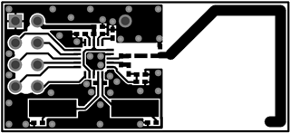
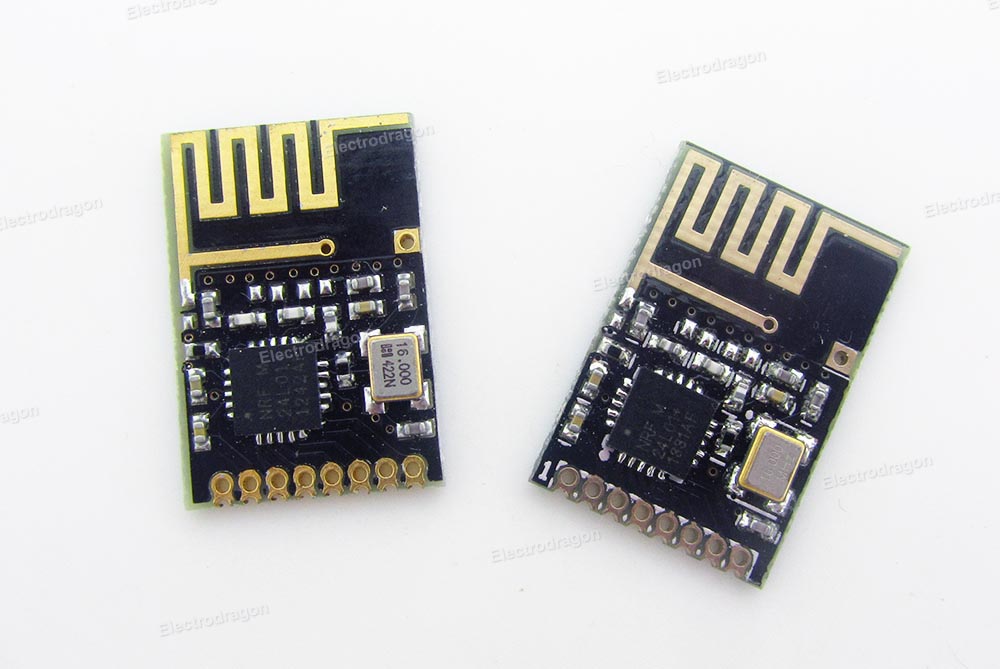
nrf24l01+, pcb mifa antenna design

Hello guys,

I tried to design a pcb antenna for a nrf24l01+, since my company doesnt allow to buy cheap smd breakout board version from china anymore
The pcb stats of the producer:

  • 2-layer FR4 1.55mm (61.023mil)  thickness, εr = 4.6
  • Copper thickness, 35μm (1.378mil)

What I used:

This results into following desgin block:


The antenna area is clear of any signals aswell as ground on top or bottom layer.

Since I have absolutly zero experience with RF antenna design I would like to have some opinions regarding my design.

Thanks so far,

Joe

Parents
  • Hey guys,

    first of all, thank you very much for your advice.
    After reading your posts and checking the files Oyvind has attached to his post I came up with following plan:

    1. Place all components and use the same size shown in the files

    2. Copy the pcb antenna

    3. Check routing

    Since I dont have very much experience with RF, as you already found out, I obviously have some (stupid) questions:

    • My pcb is a little bit thinner than the pcb used in the files. Does this have a big effect on the performance if I just use the same dimensions?
    • What about the line thickness, Antenna length etc.? I there a way to obtain the exact dimensions like width an length? Does it have to be very precise or is it not that important so I can try to measure the lines via grafic tools or something like this? This will result in little differences I guess.
  • JoE1205 said:
    I came up with following plan:

     We recommend that you copy and place the antenna first, as this is the most important part of the RF design. Keep in mind that the reference design is designed for optimal performance.

    For best result, copy the exact antenna layout with the nrf42le1, and antenna components (connected to ANT1 and ANT2). Keep space around the components and GND layer. For the antenna itself, remove any fill around and on the bottom layer.

    Then place other components and route them as wanted. 

    JoE1205 said:
    My pcb is a little bit thinner than the pcb used in the files. Does this have a big effect on the performance if I just use the same dimensions?

     No, this should be fine. Down to 0.8mm will not affect the performance.

    JoE1205 said:
    What about the line thickness, Antenna length etc.? I there a way to obtain the exact dimensions like width an length? Does it have to be very precise or is it not that important so I can try to measure the lines via grafic tools or something like this? This will result in little differences I guess.

     For the antenna and circuit, keep everything exactly the same to be on the safe side. The length of the antenna, seen in the image above, is that length in case you need to tune the antenna. See White Paper - Antenna Tuning v1.0.

    Kind regards,
    Øyvind

  • Some questions regarding the crystal.
    I cant find a crystal with +-60 ppm. Is +-50 also possible?
    The BOM is listing a HC49. Does this include any HC49/xxxx versions, for example HC49/4HSMX?

Reply Children
Related