Hi
I am reviewing the nRF52840-DK hardware documentation to make boards with good antenna performance.
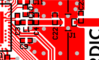
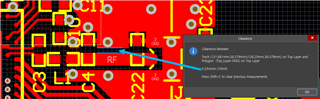
Q1. I have divided it into three areas as shown below. Is my understanding correct?

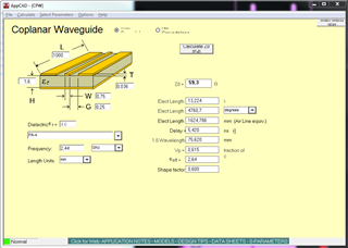
Q2. I found the following information in the document that I needed to calculate the CPWG.
Dielectric thickness = 1.4mm
Dk = 3.72
RF line width = 0.762mm
Clearance between RF line and GND = 0.254mm

I calculated the CPWG value from the link below.
http://www.rfdh.com/rfdb/cpwg.htm
The results are as follows.
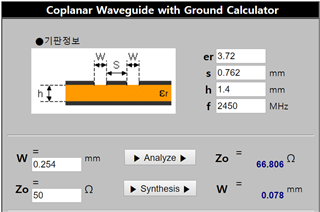
To obtain a 50 ohm line, W should be 0.078 mm. Calculated as 0.254mm according to the DK document, it becomes 66ohm.
Why is it made with 66ohm like the above?
Q3. I think the difference between 66ohm and 50ohm is compensated by C4 and C22 connected to the RF line. Am I right?
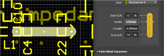
Q4. I'm going to make a 4-layer PCB (with a dielectric constant of 4.3) with 1.6T thickness. Can I make a CPWG with the same specifications as DK?
I'm looking forward to your reply.
Thanks