This post is older than 2 years and might not be relevant anymore
More Info: Consider searching for newer posts

Flexible PCB design for 18650

Hi,

as my project moves forward I've switched to development of central board. In addition to space restrictions the board is promising to be a resource hog. A 2500+ mAh battery is a must, and after some review I chose 18650 as cheap and compact solution. However, due to number of components an FR4 board doesn't fit the size well. After number of unsuccessful attempts I've started to consider fully flexible PCB for my design. Again, as with the peripheral part the RF is something which must be considered in the first place. To keep things weirder I'm planning to put antenna and nRF52832 on different parts of the board :-)

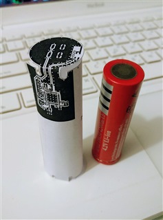
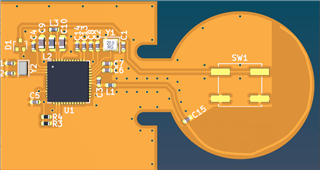
So here is the design: take a 18650 battery, wrap the board around it, then cover battery ends with leafs from the same FPCB. The leafs should have a stiffener. In order to assemble the thing add two plastic caps on the battery - they will align main board and fix the leafs. The result cylinder may be placed inside aluminum tube and sealed with two external plastic caps. Because of the tube the only shield free areas on the device are the ends. Such my antenna (and button) were placed on one of the leafs, and MCU resides on the main board:

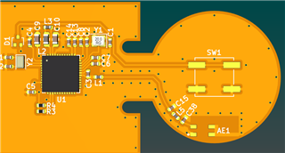
I requested exact specs for materials used in manufacturing process, still wait for reply. For the draft I assumed adhesiveless 75 um polymide, 1 oz/sq.ft copper which resulted in 0.17 mm track width to match 50 Ohm impedance. The antenna in subject is Johanson 2450AT18D0100.

And if you won't mind a number of questions, of course:

  1. Although the idea to employ FPCB isn't new, what do you think about the proposed design? Is it prone to RF issues? What may be recommendations to it?
  2. It looks like there is plenty of space for a radial monopole, but I'm concerned about the button in the same area. Taking in account the battery would it be better to stick with a chip antenna anyway?
  3. As a followup to the previous question, because of the battery should I look for a zero clearance chip antenna instead? Like the Johanson 2450AT42E0100. It has worse gain and seem will require some cheating like no ground on bottom layer and use battery negative for that kind.
  4. The matching network for the nRF52832 is a replica of the reference design. For flexible PCB component values have to be adjusted. Would it be possible to do with your help?
  5. Another question is should I tweak tracks width as well? In particular, connection between C3 and L1 doesn't look right to so thin substrate.

Gerber files attached. The circuit (and hence designators) were copied from the reference design (the only difference: R3 and R4 are I2C pullups, please ignore; D1 is used to share the SW1 button between nRF52 and battery management IC).

Thank you!

rnc1cc9a.zip

Parents
  • Hi Mike, 

    I have to look more into this case tomorrow, but I few questions:
    1. Is the pcb more then two layers? 
    - I only found two layers in the gerber files, and some routing seems to be missing
    2. What is the radius of the battery, and what is the radius of the edge of the pcb, where the antenna is sitting? 
    3. Will the battery be connected to the pcb edge where the antenna is, or will it be some distance to the antenna? From what your writing I think no clearance, but I want to be sure. 

    The matching network for the nRF52832 is a replica of the reference design. For flexible PCB component values have to be adjusted. Would it be possible to do with your help?

     - Of course, see the old case, https://devzone.nordicsemi.com/f/nordic-q-a/49686/optimizing-pcb-space-with-footprint-size, I can help you with tuning! 

    Another question is should I tweak tracks width as well? In particular, connection between C3 and L1 doesn't look right to so thin substrate.

     - The track width track that is important to change is the one from L1 to the antenna, this needs to be 50 Ohm. Calculate based on you substrate. 

    Best regards,
    Kaja

Reply
  • Hi Mike, 

    I have to look more into this case tomorrow, but I few questions:
    1. Is the pcb more then two layers? 
    - I only found two layers in the gerber files, and some routing seems to be missing
    2. What is the radius of the battery, and what is the radius of the edge of the pcb, where the antenna is sitting? 
    3. Will the battery be connected to the pcb edge where the antenna is, or will it be some distance to the antenna? From what your writing I think no clearance, but I want to be sure. 

    The matching network for the nRF52832 is a replica of the reference design. For flexible PCB component values have to be adjusted. Would it be possible to do with your help?

     - Of course, see the old case, https://devzone.nordicsemi.com/f/nordic-q-a/49686/optimizing-pcb-space-with-footprint-size, I can help you with tuning! 

    Another question is should I tweak tracks width as well? In particular, connection between C3 and L1 doesn't look right to so thin substrate.

     - The track width track that is important to change is the one from L1 to the antenna, this needs to be 50 Ohm. Calculate based on you substrate. 

    Best regards,
    Kaja

Children
  • Hi Kaja!

    1. Is the pcb more then two layers? 
    - I only found two layers in the gerber files, and some routing seems to be missing

    The board has two layers indeed. I just didn't route all of the schematic, but the MCU and antenna only because they're most questionable to me at the moment on this flex board. Upon your approval I'll finish the layout, of course.

    2. What is the radius of the battery, and what is the radius of the edge of the pcb, where the antenna is sitting?

    Battery diameter is 18 mm, length is 65 mm. Diameter of the PCB edge leaf is 22 mm.

    3. Will the battery be connected to the pcb edge where the antenna is, or will it be some distance to the antenna? From what your writing I think no clearance, but I want to be sure. 

    I think it will be soldered straight into the board somewhere in the middle of main area. Please take a look at the first 3D picture - it has bounding box for a 18650 battery. Solder points will be right at solder tabs of the battery (which looks like this). However, the board will be bent around it and therefore clearance from antenna to negative pole (the closest one) will be around 5 mm.

    It's gonna be something like this (sorry, have no battery with pads):

     - The track width track that is important to change is the one from L1 to the antenna, this needs to be 50 Ohm. Calculate based on you substrate. 

    Yeah, I've calculated it in my post above. Set to 0.1 mm for now. This constrained me to 1/2 oz/sq.ft copper which brought some power issues (the battery charge/discharge current is around 3A), but that's different story. Anyway, any ideas on how to manage this are welcome :)

    Yours,

    Mishka

  • Hi Mishka, 

    so to calculate the width you should use a calculator for a coplanar waveguide:

    Because the distance to ground on the sides also affect the impedance, you can adjust both the width and distance to ground so that you get a width that is more suited. 


    • It looks like there is plenty of space for a radial monopole, but I'm concerned about the button in the same area. Taking in account the battery would it be better to stick with a chip antenna anyway?
    • As a followup to the previous question, because of the battery should I look for a zero clearance chip antenna instead? Like the Johanson 2450AT42E0100. It has worse gain and seem will require some cheating like no ground on bottom layer and use battery negative for that kind.

     
    It's difficult to say, without measuring, I would recommend you to make one prototype with a monopole antenna and one with the chip antenna, I can help you with tuning, and then you can check performance. 
    5 mm to the battery is the minimum distance we recommend and will probably be okay, but it's always difficult to say how much a battery will affect the antenna, but we can always try to tune away the affect from the battery and especially  the enclosure in this case. 
    The zero clearance chip antenna is difficult to tune, and I would recommend that you try the two other alternatives. 
    What is your requirement for range? 

    For the monopole antenna, try something like this and have a look at our whitepaper on how you should make the antenna: 


    You can move forward in you deign process, and I can have a new look at the schematic and layout when you are ready for a second review. 

    Best regards,
    Kaja

  • Hi Kaja,

    thank you a lot for the review! It really cleared the mess for me.

    Well, this particular device is better to reach a long distance (many tens of meters if not further), but 95% of time it will work within just couple of meters. So in 95% cases the prototype will forgive me my antenna design mistakes I hope :-)

    For now I'll skip the zero clearance solution, thanks for the tip. I do also very appreciate your note about the coplanar waveguide. First, it prevented me from screwing up the RF. Second, it saved me a day due to copper layer of normal thickness (heh, it was tricky to route 2A tracks on 0.5 oz foil).

    Here is the 50 Ohm impedance feed line, with bottom ground plane:

    • Substrate dielectric constant - 3.4 (polyimide)
    • Substrate thickness - 65 um (from PCB service)
    • Copper thickness - 35 um (1oz/sq.ft)
    • Track width - 0.17 mm (approx 35 um * 5)
    • Track clearance - 0.54 mm (calculated)

    So, I'll route the board. For the very first time I'll stick with a chip antenna, just to eliminate some of unknowns. The monopole antenna whitepaper is very pragmatic, nice. I'd want to give it a try in the next round. Okay, hope to get back to you with complete PCB and schematic within a week.

    Thank you once more for your help!

    Yours, Mishka

  • Hi Mishka, 

    I'm glad to hear that I could be of help! 

    Looking forward to seeing the design. 

    Best regards,
    Kaja

Related