This post is older than 2 years and might not be relevant anymore
More Info: Consider searching for newer posts

nRF52840 Shifted signal radio.

Hi everyone,

We need your help with a condition that we encountered in our prototype of a nRF52840 that use a ceramic antenna. Our current design is poor and we will have migrate eventually to the PCB trace antenna. But we need to understand whats going on here. Our design was based on the hardware documentation of Nordic "nrf52840_qiaa_var5_schematic.pdf" with a little twist in order to use a ceramic antenna, keeping the LC matching components as you can see int the schematic design.
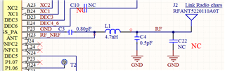
Current design

Schematic design.

Board design}

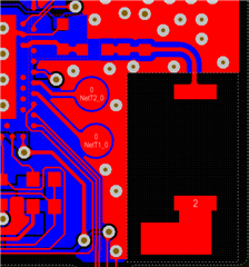
Board PCB Design, 2 layers, 1.6mm height.

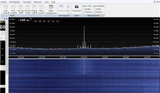
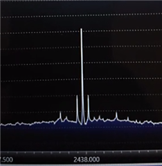
We run the board with a Radio firmware tuned on 2.438 GHz and we see the signal with a lot of harmonics but also shifted, and this is the actual issue that we need to understand. We compare the nRF52840DK board with our design, and the difference are obvious.

EBoard

nRF52840DK with radio test 2.438 GHz

Prototype

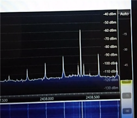
Prototype board  with radio test 2.438 GHz

Can you help us with any observation or if you found other cases or design with similar behavior? 

PD: Sorry for the quality of the screenshots.

Thanks in advance.

Rvc.

Parents
  • Hi,

    I have a couple of questions and comments regarding your design:

    • Has the design been reviewed and tuned?
    • What output power are you using?
    • Chip antennas should have a full Pi network for achieving good impedance matching.
    • You should not have a trace in the layer under C3, instead, you should have a solid gnd layer.
    • Are you doing a conductive or radiated measurement?

    regards

    Jared 

Reply
  • Hi,

    I have a couple of questions and comments regarding your design:

    • Has the design been reviewed and tuned?
    • What output power are you using?
    • Chip antennas should have a full Pi network for achieving good impedance matching.
    • You should not have a trace in the layer under C3, instead, you should have a solid gnd layer.
    • Are you doing a conductive or radiated measurement?

    regards

    Jared 

Children
  • Hi Jared,

    Thanks for replying, 

    • Q1: This is the first design has not be tuned yet. 
    • Q2: Default, 4db.
    • Q3: Yes we understand that, actually we will modify this in the near future. 
    • Q4: This also was pointed by our design team.
    • Q5: We dint understand your question, but we are measuring the signal behavior with an spectrum analyzer.

    Regarding the poor matching circuit for the CHIP Antenna, with our poor design we should see attenuation and harmonics but i don't know why the signal is shifted in the spectrum analyzer?

  • Hi,

    The shifting can be due to the Cl of the crystal not fitting the parallel load capacitors. 

    • What is the model number of your crystal, and what size are the load parallel capacitors?
    • Could you upload both schematic and layout of your design?
    • You can use the spectrum analyzer and try to decrease and increase the parallel load capacitors of the crystal and see if the signal is shifted down/up in frequency.
    • What is the distance between each peak?

    regards

    Jared 

  • Hi Jared,

    Thanks for the answer, we are currently replacing the crystal capacitors, in order to check this issue. In the mean time The crystal is FA-128-320000MF10Z-AJ3 and the capacitors have 12pF for C1 = C2. The layout and schematic it will be upload later. 

  • Hi Jared,

    We solve our issue, finally following some our your instructions. It was a poor soldering of one of the capacitors. We confirm this while changing the crystal capacitor, one of them was solder wrong.  After we solder properly this capacitor we run the radio test and the programmed radio signal match measure signal.

    Thanks for your time and advice's!

    Regards!

    Ricardo V.

Related