This post is older than 2 years and might not be relevant anymore
More Info: Consider searching for newer posts

nrf9160 SPI reading problems

Hello,

i'm trying to use SPI with nrf9160DK as master and RFM96 module as slave. At the moment, i'm developing elementary functions to write and read from my slave device. RFM9X module needs the following settings:

Word size: 8bit, CPOL=0, CPHA=0, Max SPI bus Frequency = 10MHz, CS Active Low, MSB first

The SPI timing sequence for a standard single access is the following:

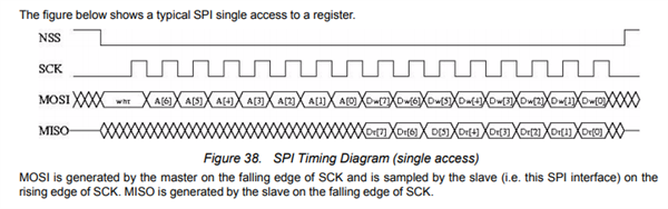
The MSb of the address byte needs to be 1 if i'm writing, 0 if i'm reading the register.

The pin used in this test are placed in overlay file:

&spi3 {
	status = "ok";
	sck-pin = <10>;
	mosi-pin = <11>;
	miso-pin = <12>;
	spi-max-frequency = <2000000>;
};

I used VDD=3V using SW11 of the nrf9160DK. I verified that SPI is generally working using a loopback test. I verified all the connections from the slave side.

This is the code i developed:

#include <zephyr.h>
#include <sys/printk.h>
#include <drivers/spi.h>
#include <stdlib.h>
#include <device.h>
#include <drivers/gpio.h>


#define SPI_READ_REGISTER 0x00      //0   - most significant bit = 0
#define SPI_WRITE_REGISTER  0x80    //128 - most significant bit = 1

#define GPIO_CS 13

struct device * spi_dev;
struct device *CS_dev;

struct spi_config spi_cfg = {
	.operation = SPI_WORD_SET(8) | SPI_TRANSFER_MSB,  //CPOL=0, CPHA=0
	.frequency = 2000000,  //Max RFM96 speed is 10MHz
	.slave = 1,
};


struct device* spi_init(struct spi_config * spi_cfg) {
  struct device *spi_dev;
  
  const char* const spiName = "SPI_3";
  spi_dev = device_get_binding(spiName);
  if (spi_dev == NULL) {
    printk("Could not get %s device\n", spiName);
  }
  return spi_dev;
}


int spi_read_test(struct device * spi_dev, const struct spi_config * spi_cfg, 
                                                          u8_t reg_addr, u8_t * rx_data) {
  
  int err;
  
  //create the tx buffer - i need to send on MOSI the register address i want to read
  u8_t tx_buf[1]={SPI_READ_REGISTER|reg_addr};

  const struct spi_buf spi_tx_buf = {
	.buf = tx_buf,
	.len = sizeof(tx_buf),
  };
  const struct spi_buf_set tx = {
	.buffers = &spi_tx_buf,
	.count = 1,
  };
  
  //write data on spi bus
  err = spi_write(spi_dev, spi_cfg, &tx);
  if (err<0) {
    return err;
  }

  //build spi_buf_set element for read
  const struct spi_buf spi_rx_buf = {
	.buf = rx_data,
	.len = 1,
  };
  const struct spi_buf_set rx = {
	.buffers = &spi_rx_buf,
	.count = 1,
  };

  err = spi_read(spi_dev, spi_cfg, &rx);
  return err;
}


void main(void)
{
  printk("Debug SPI test\n");

  //Configure CS device and behaviour
  CS_dev = device_get_binding(DT_GPIO_P0_DEV_NAME);
  gpio_pin_configure(CS_dev, GPIO_CS, GPIO_DIR_OUT);
  gpio_pin_write(CS_dev, GPIO_CS, 1); //PULL CS HIGH


  //Init spi device (actually pin for CS is useless and it is driven manually)
  spi_dev = spi_init(&spi_cfg);

  k_sleep(3000);

  u8_t rx_data=0;
  u8_t reg_addr=0x01;
  gpio_pin_write(CS_dev, GPIO_CS, 0);   //PULL CS LOW
  spi_read_test(spi_dev,&spi_cfg, reg_addr,&rx_data);  //i want to read register address 1
  gpio_pin_write(CS_dev, GPIO_CS, 1);   //PULL CS HIGH
  
  printk("Written to reg address: %d\n", reg_addr);
  printk("Register value: %d\n",rx_data);

}

With this code i'm unable to get any consistent answer from my slave device (i noticed that i get always 8 or 0 if the address i use is even/odd...doesn't make any sense). This is a first bunch of fast questions about SPI:

- Is the spi config structure correctly set or i missed anything? In particular i want to be sure that i understood CPOL and CPHA setting;

- What about the "slave" element of spi config structure? I have 1 slave so i suppose i had to set it to 1, but is it really necessary?

- I'm having hard time getting a full grasp about "spi_buf" and "spi_buf_set" structure. While is intuitive understanding why "spi_buf" is structured like this, i don't understand why "spi_buf_set" has a "count" element. Why should i set an array or spi_buf struct?

- Is, in general, the flow described in the above picture reproduced by my code or i am missing anything?

Thanks,

Frax

  • Hi,

    This is somewhat similar to this case:
    https://devzone.nordicsemi.com/f/nordic-q-a/60531/clarification-about-spim---ss-pin-management-for-nrf9160

    To be able to debug this further you will need an logic analyzer trace, I can highly recommend https://www.saleae.com/, then you can observe all data pins and see exactly how the configuration will change the transfer. You can also upload the trace for us to open here. At the moment the problem may be anything (even electrical), so getting a trace is a good next step. 

    Best regards,
    Kenneth

  • Hi Kennet,

    thank you for your answer. Going in order:

    I well know this post, considering i'm the one who wrote it Slight smile

    so getting a trace is a good next step. 

    My bad for not being totally clear about this. I have no logic analyzer, but i'm using a digital oscilloscope, so i'm confident that signals are going.

    Purpose of the ticket was being sure that i had no code issues. By the way, taking my time to perform some "trial and error" test i'm able to address most of my questions now. Leaving the answers here for the purpose of sharing:

    - Is the spi config structure correctly set or i missed anything? In particular i want to be sure that i understood CPOL and CPHA setting;

    Yes, it is set correctly. In particular, SPI_MODE_CPOL and SPI_MODE_CPHA means respectively "Set SPI CPOL = 1" and "Set SPI CPHA=1". Not setting, of course, means the opposite.

    - What about the "slave" element of spi config structure? I have 1 slave so i suppose i had to set it to 1, but is it really necessary?

    Seems not. I didn't find any problem in changing slave from 0 to 1 and back. I don't know what's the purpose. Maybe Kenneth can make clear this point?

    I'm having hard time getting a full grasp about "spi_buf" and "spi_buf_set" structure. While is intuitive understanding why "spi_buf" is structured like this, i don't understand why "spi_buf_set" has a "count" element. Why should i set an array or spi_buf struct?

    It can be generally useful when using multi slave. My bad for not thinking enough...

    Is, in general, the flow described in the above picture reproduced by my code or i am missing anything?

    This is a critical point. No, the code i described doesn't work. This is the correct code:

    int spi_dev_read(struct device * spi_dev, const struct spi_config * spi_cfg, 
                                                              u8_t reg_addr, u8_t * rx_data) {
      
      int err=0;
      
      //create the tx and rx buffer
      u8_t tx_buf[1]={SPI_READ_REGISTER|reg_addr};
      u8_t rx_buf[2];
    
      const struct spi_buf spi_tx_buf = {
    	.buf = tx_buf,
    	.len = sizeof(tx_buf),
      };
      const struct spi_buf_set tx = {
    	.buffers = &spi_tx_buf,
    	.count = 1,
      };
    
      const struct spi_buf spi_rx_buf = {
    	.buf = rx_buf,
    	.len = sizeof(rx_buf),
      };
      const struct spi_buf_set rx = {
    	.buffers = &spi_rx_buf,
    	.count = 1,
      };
      err = spi_transceive(spi_dev, spi_cfg,&tx, &rx);
      *rx_data = rx_buf[1];  //first byte is dummy, second one is the correct result
      return err;
    }

    Please note that this time i used transreceive and not spi_write + spi_read. This is because when used the spi_cs_control structure as pointed here  both spi_write and spi_read pull low (at the beginning) and high (at the end) of the function at the end of the function, while many spi devices want that write (register address) and read (register value) happen in the same transaction. This can be obtained even using SPI_HOLD_ON_CS option, but i think is more efficient this way.

    I'm leaving the ticket open for further comments of Kenneth. I will close it in a few days if no comment come.

    Best,

    Francesco

Related