This post is older than 2 years and might not be relevant anymore
More Info: Consider searching for newer posts

PCB Antenna connection of nRF52810

Dear Nordic user,

We are under development with nRF52810-QCAA.

The first board has been make and is being tested.

However, after making the board, I noticed that the important part mentioned in the datasheet was not applied.

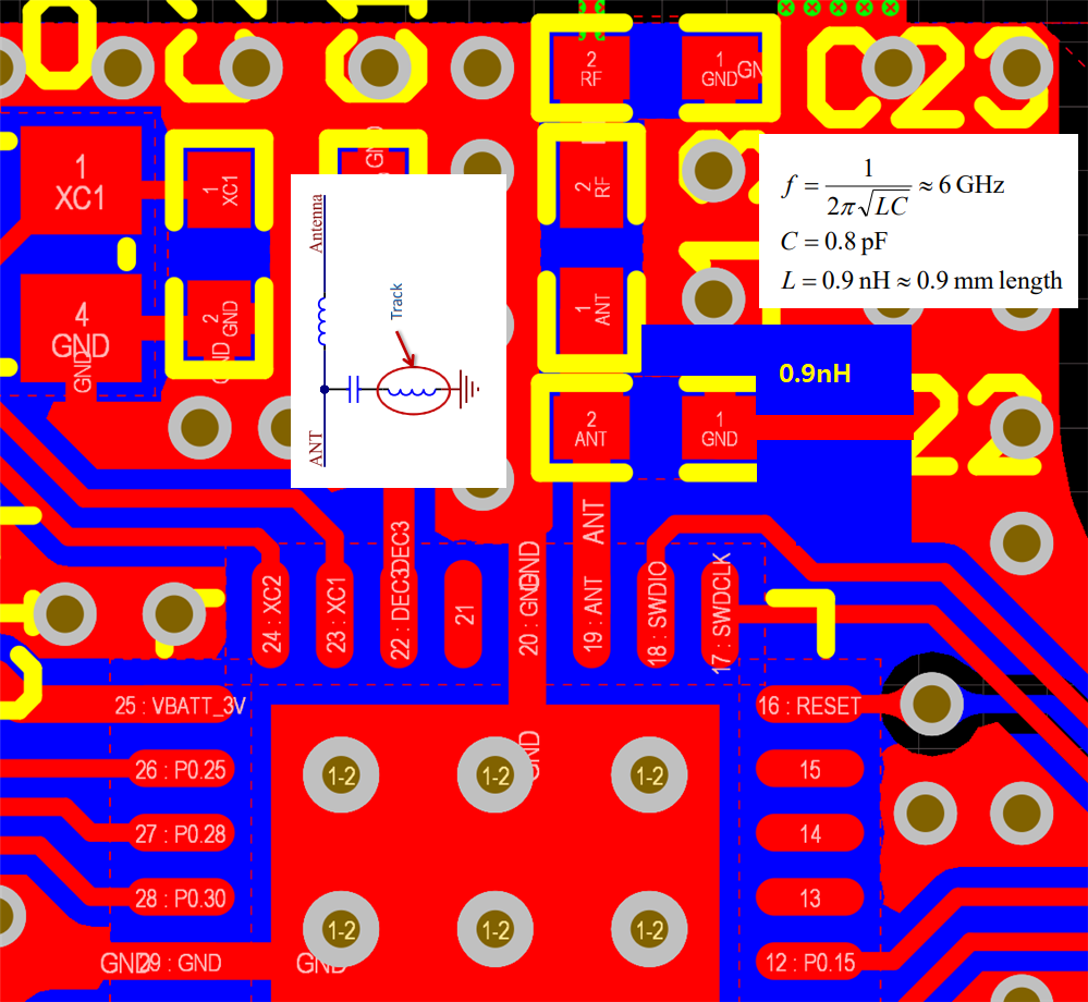
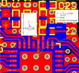
It is the important information (comment in the blue box) mentioned in 7.3.9 PCB layout example of nRF52810_PS_v1.3.pdf.

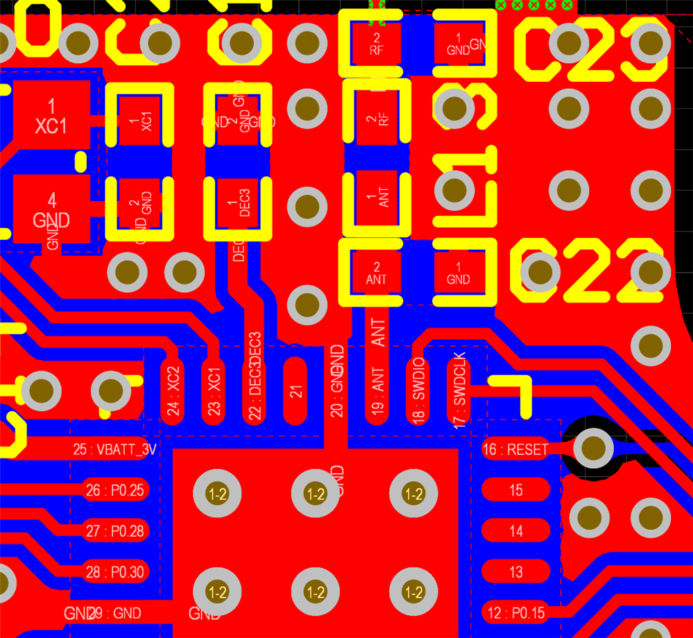
Below is the antenna connection screenshot of our board.

GND is directly connected to the nRF52810's 20 pin, and C22 is connected to the other GND.

 - component value are C22/0.8pF, L13/3.9nH, C23/N.C

I’m not sure how much this affects the harmonic filtering and whether we should take the risk of not passing regulation tests. 

1. Is this an important comment that must be followed? -  in 7.3.9 PCB layout example of nRF52810_PS_v1.3.pdf

  1.1 Please explain the situation that may occur if I do not follow the important comment.

2. If not, what steps should I take to improve other than modifying the PCB?

3. What instruments or specifications are needed to perform the procedure?

4. Is the best way to change the PCB design?

Thanks in advance for your answer.

Sungsuk Han.
Parents
  • Hi,


    See the explanation here: nRF52 matching network.pdf

    Without this harmonic filtering will be degraded, and you might fail regulatory requirements for unwanted emissions. You might be able to tune the filter by adjusting C3 and L1 slightly, but you risk having to lower the output power to pass the requirements. You might still have to tune C3 and L1 slightly, but this will be much easier and generally result in better performance in the end. We therefore recommend that you ground C3 this way if possible, in your current layout I do not see any reason not to do this.


    Best regards,
    Andreas

  • Hi, Andreas.

    Thank you very much for your answer.

    I have questions.

    1. According to the contents of your attachment, can you see the same effect if we connect the GND and C22(our pcb design) with the length (about 0.9mm) and width(about 0.25mm) shown in the nordic reference design?

    2. If not, I have to follow the reference design due to the special features of Pin 20/VSS? \

    Thank you and Best Regards,

    Sungsuk Han.

  • Hi,


    1. It might not be that simple, the track as described in the attachment leads into the radio (pin 20, GND), whereas in your design there is still some distance between what you define as 'ground' and the same point inside the radio. Impossible to say what effect this will have.

    2. I strongly recommend you do so, this has been verified for 5+ years and there is nothing keeping you from replicating this. Your other alternative will probably work, but you will likely get a harder time tuning the filter, worst-case having to sacrifice some performance for compliant harmonic emissions, but why risk it.


    Best regards,

    Andreas

Reply
  • Hi,


    1. It might not be that simple, the track as described in the attachment leads into the radio (pin 20, GND), whereas in your design there is still some distance between what you define as 'ground' and the same point inside the radio. Impossible to say what effect this will have.

    2. I strongly recommend you do so, this has been verified for 5+ years and there is nothing keeping you from replicating this. Your other alternative will probably work, but you will likely get a harder time tuning the filter, worst-case having to sacrifice some performance for compliant harmonic emissions, but why risk it.


    Best regards,

    Andreas

Children
Related