Hello,
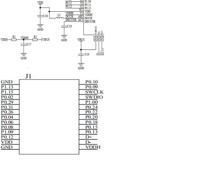
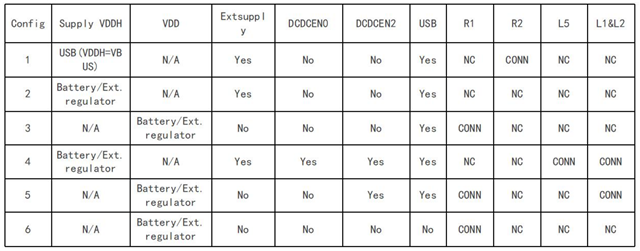
For our project we were planning on using a 3rd party module MS88SF2 (nRF52840), which schematic snapshot is provided and which will be powered though the li-po battery. Full documentation is available here. What confused me was power configuration they selected to use which I couldn't identify from any of the given examples on the design references (starting page 688). If I understand it right, the way how the chip module operates is as follows:
If 3.3V is applied to VDD, then VDDH = VDD due to resistor R1 and the chip thus enters “Normal Voltage Mode”, where REG0 is not used. If 5V is applied to VDDH, the chip goes into “High Voltage Mode” and then DCDC converter is used to set VDD to be some lower voltage e.g. 3.3V. The implications though will be that current will flow from VDDH to VDD, which depends on the resistor R1. At the same time VBUS = VDDH due to connected resistor R2 and the USB module gets powered together with the chip, thus allowing to program the chip through the USB. The take away is that when powering from the battery, use a 3.3V regulator to provide correct voltage on VDD, however when on USB, use 5V on VDDH, which will consume slightly more power due to the current flowing through the resistor R1. Is that correct and do you think that the configuration they chose will not have any further implications to the way how the module operates? I also contacted the supplied as they did not provide R1 and R2 values..
I hope you will be able to help me even though this is a 3rd party module, thanks!


