This post is older than 2 years and might not be relevant anymore
More Info: Consider searching for newer posts

Custom PCB with the NRF52840: Programming, Antenna, USB, and Crystal

Hi,

I'm making a custom board with NRF52840 and would like to confirm some schematic/layout considerations for things I couldn't quite find in other posts. I apologize if these are naive questions - hopefully I can get my final answers here!

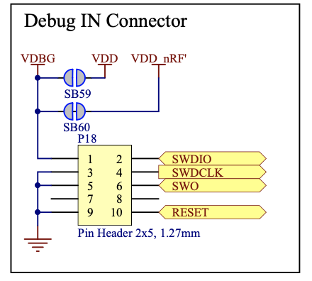
  1. How can I program the NRF52840 when it's on my own board? Other posts have said that it's as simple as using an nrf52 dev kit as an external debugger and connecting the SWDIO, SWCLK, VDD, and GND pins (https://devzone.nordicsemi.com/f/nordic-q-a/30127/programming-custom-pcb-nrf52840). Is there any initial set up I have to do in addition? I also have access to a Jlink debugger, is it possible to use that as an external debugger with the nrf52840? 
  2. I'd like to use the NRF52840's 2M bluetooth! I've opted for an integrated chip antenna (the same as the thingy52 - see fig 5: link) and then cobbled together impedance matching networks based off of another devzone post. The thing that confuses me is that the Thingy52's antenna-side matching network is missing an inductor to ground (even though it's suggested on the manufacturer's data sheet). The response, however, actually says that you should have it. When it comes to the nrf52840-side impedance matching network I got a little confused because there are different component values in different designs (the dev kit schematic uses different components than the reference designs in/around Figure 212 in the data sheet). Shouldn't the network always be 50 ohms? Is there a single recommendation for a matching network on the nrf-side? I can post a screen shot of my antenna schematic if it would help!
  3. Is it okay if VDDUSB is powered while VDD isn't on the nrf52840? I'm trying to find potential power sequencing faults. VDDUSB just goes into a level shifter inside the nrf52840 I assume - is that a fair assumption?
  4. I couldn't find the exact crystal used in the dev kit design. Is it alright to use this similar crystal from digi-key? I know it seems like a silly question but I've always been taught that parasitics can kill a crystal configuration so I'm worried. It'll probably be fine ... but hey, I'm worried.

Thank you so much for any/all help given. Having these questions answered will help me sleep better at night!

  • Hi,

    Answers to your questions:

    1. The nRF52 is programmed through the SWD interface which uses a SWDCLK line and a SWDIO line. You would need to route VDD and GND in addition to the SWD data and clock lines to a header (to make them externally available for a debugger). J-link is the debugger that we officially support so good choice. Also, our nRF52 DKs and nRF52840 DKs comes with an external debugger that can be used for programming custom boards. If you take a look at the schematic of the nRF52840 DK then you'll see that the SWD pins are routed to the onboard interface chip which acts as a onboard debugger.
    2. The recommended values are just what we recommend as a starting point. You would either way at some point have to tune the matching network. Every matching network has to be adjusted (tuned) for that specific PCB. Thus, given that the nRF52840 DK and the Thingy are two different boards, then they would require two different matching networks. It seems that the misunderstanding is because you've assumed that the nRF52832 (which is the IC used on the Thingy:52) and the nRF52840 uses the same matching network for the radio. They don't! The matching network for the nRF52832 radio consists of a parallel capacitor and a series inductor seen from the radio. The matching network for the nRF52840 depends on the package but in most cases consists of a Pi-network + a parallel capacitor seen from the radio. To conclude, the Thingy:52 which uses nRF52832 has therefore the correct matching network as C3 and L1 is the matching network for the radio, while the C13, L5, L4 is the T-network for the antenna as described in it's datasheet. 
    3. The nRF52840 won't get hurt if you only power the USB interface but it would need to be powered through VDDH/VDD for the IC to actually work.
    4. The crystals that they use on the nRF52840 DK is NX3215SA-32.768K-STD-MUA-9 and MP06003 and is listed in the BOM file. 

    Note: You can make a new ticket with your design files (schematic + Gerber/Altium files)  for a review of your design from us!

    Hope this helps with the sleep Slight smile

    best regards

    Jared

  • Sorry for the late reply - I forgot to say thank you because your message was such a relief. Thank you!

    I just have a clarifying question: I assume this is the J-link debugger port on the dev kit:

    I will submit another ticket with my schematic and layout to get a quick review from you guys! That'd be amazing. 

    Thanks for all your help,

    Ryan

Related