This post is older than 2 years and might not be relevant anymore
More Info: Consider searching for newer posts

i2c drive strength unsolved after applying forum's method

Hi Devzone:

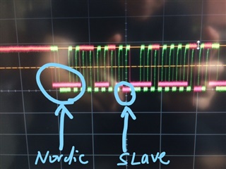
I am using P0.00 as SDA and P0.01 as SCL on nRF52833, And I got waveforms like below when I am doing I2C transactions:

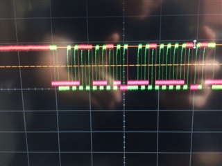
the red waveform is SDA and the green waveform is SCL.

As shown in the picture the nordic chip doesn't pull the SDA line (red) all the way down to voltage zero when it's 0.

We already have 1.8V and a pull up resistor of 1.8K ohm on both pins.

I looked at twi config settings (nrf_drv_twi_config_t), there's no where to set drive strength, only frequency, interrupt_priority and clear_bus_init.

So I added the following code to gpio_init():

nrf_gpio_cfg(CD_AUD_SDA,
NRF_GPIO_PIN_DIR_OUTPUT,
NRF_GPIO_PIN_INPUT_CONNECT,
NRF_GPIO_PIN_NOPULL,
NRF_GPIO_PIN_H0D1,
NRF_GPIO_PIN_NOSENSE);
 nrf_gpio_pin_set(CD_AUD_SDA);

I played around nrf_gpio_pin_drive_t with H0H1,  H0D1 and some other permutations, It didn't solve the SDA not driven to zero voltage problem. The waveform is still the same as shown previously.

And adding this code sometimes locks up the program.

So what's the right way to solve the SDA not driven to zero voltage problem? 

Thanks.

Parents
  • Hi,

    Is zero volt a requirement for your application? A logical '0' is defined as minimum VSS and maximum VSS+0.4V for GPIOs according to the GPIO Electrical Epecification in the nRF52833 Product Specification. What is the voltage level of your logical '0' measured against VSS?

    Best regards,

    Håkon

  • Hi helsing:

    Yes we want a close zero. Currently that "zero voltage" on SDA is 0.24V.

    If you examine my waveform closely, you will find that the SDA was driven to close zero better by the slave device compared to when the Nordic chip was driving it. see my picture below:

    Also SCL (green line) is able to drive to close to zero just fine.

    This means the Nordic chip should be able to do better driving SDA to zero.

    I am also asking if what I did in the code is the right approach to the problem. 

    So to recap my question:

    Beside writing nrf_drv_twi_config_t (as shown below):

        nrf_drv_twi_config_t const twi_config0 = {
           .scl                = CD_AUD_SCL,
           .sda                = CD_AUD_SDA,
    
           .frequency          = NRF_DRV_TWI_FREQ_100K,
           .interrupt_priority = APP_IRQ_PRIORITY_MID,
           .clear_bus_init     = false
        };

    Do we still need to write nrf_gpio_cfg (as seen below) to further define I2C SDA and SCL pins (driving strength, pull up etc)?

    nrf_gpio_cfg(CD_AUD_SDA,
    NRF_GPIO_PIN_DIR_OUTPUT,
    NRF_GPIO_PIN_INPUT_CONNECT,
    NRF_GPIO_PIN_NOPULL,
    NRF_GPIO_PIN_H0D1,
    NRF_GPIO_PIN_NOSENSE);
     nrf_gpio_pin_set(CD_AUD_SDA);

    because without nrf_gpio_cfg (#2 code block), the bus still works, just with that logic 0 driving to non zero problem I mentioned.

    And with nrf_gpio_cfg (#2 code block) in the code, there's no effect on alleviating logic 0 driving to non zero problem.

    Again we need the bus to drive to close zero. The current i2c driving is unacceptable in our applications.

    So is there any other way to solve non zero driving problem?

    Thanks.

Reply
  • Hi helsing:

    Yes we want a close zero. Currently that "zero voltage" on SDA is 0.24V.

    If you examine my waveform closely, you will find that the SDA was driven to close zero better by the slave device compared to when the Nordic chip was driving it. see my picture below:

    Also SCL (green line) is able to drive to close to zero just fine.

    This means the Nordic chip should be able to do better driving SDA to zero.

    I am also asking if what I did in the code is the right approach to the problem. 

    So to recap my question:

    Beside writing nrf_drv_twi_config_t (as shown below):

        nrf_drv_twi_config_t const twi_config0 = {
           .scl                = CD_AUD_SCL,
           .sda                = CD_AUD_SDA,
    
           .frequency          = NRF_DRV_TWI_FREQ_100K,
           .interrupt_priority = APP_IRQ_PRIORITY_MID,
           .clear_bus_init     = false
        };

    Do we still need to write nrf_gpio_cfg (as seen below) to further define I2C SDA and SCL pins (driving strength, pull up etc)?

    nrf_gpio_cfg(CD_AUD_SDA,
    NRF_GPIO_PIN_DIR_OUTPUT,
    NRF_GPIO_PIN_INPUT_CONNECT,
    NRF_GPIO_PIN_NOPULL,
    NRF_GPIO_PIN_H0D1,
    NRF_GPIO_PIN_NOSENSE);
     nrf_gpio_pin_set(CD_AUD_SDA);

    because without nrf_gpio_cfg (#2 code block), the bus still works, just with that logic 0 driving to non zero problem I mentioned.

    And with nrf_gpio_cfg (#2 code block) in the code, there's no effect on alleviating logic 0 driving to non zero problem.

    Again we need the bus to drive to close zero. The current i2c driving is unacceptable in our applications.

    So is there any other way to solve non zero driving problem?

    Thanks.

Children
  • Hi Cheng

    Sorry for the slow response. Håkon is on vacation at the moment, and I will handle your case in the mean time. 

    Are you using the nRF52833DK for this test, or some other hardware or module?

    The P0.00 and P0.01 pins are connected to the external 32K crystal on the DK, and it is possible that this connection is interfering with your signals. 

    Have you tried to use some other pins, such as P0.02/P0.03, for the I2C interface?

    Alternatively you can disconnect P0.00 from the 32K crystal by cutting solder bridge SB2, and soldering SB4. 

    Best regards
    Torbjørn

  • Two comments might help improve this. First the nrf_gpio_cfg() to change the SDA pin to H0D1 has to be invoked after setting up the I2C, not before, as the i2c (twi) init will overwrite the H0D1 settings with low-drive S0D1.

    Second when using the (slow) i2c/twi clock speed of 100kHz a pull-up on SDA of 1k8 is overkill; that pull-up could be changed to (say) 4k7. Such a change would improve the low-level if correctly setting H0D1 doesn't get the level low enough to meet your requirements.

    Why does the slave device perform better than the Nordic device? Because if it is a dedicated i2c/twi chip it has much higher drive capability as it was designed to only drive SDA whereas the Nordic is a general purpose i/o pin allowing use of any pin for SDA  (unlike some other MPUs which might have dedicated drive pins which can't be changed).

    Setting H0D1 after the i2c/twi init allows use of a pull-up as low as 1k0 at 400kHz, by the way. 'course, the lower the pull-up resistor value the more the coin cell has to supply in a case where longevity is required.

Related